Cologne Chip – GateMate
Germany
The GateMateTM FPGA family of Cologne Chip AG addresses all application requirements of small to medium size FPGAs. Logic capacity, power consumption, package size and PCB compatibility are best in class. GateMateTM FPGAs combine these features with lowest cost in industry making the devices well suited from University projects to high volume applications. Because of the outstanding circuit size/cost ratio, new applications now can use the benefits of FPGAs.
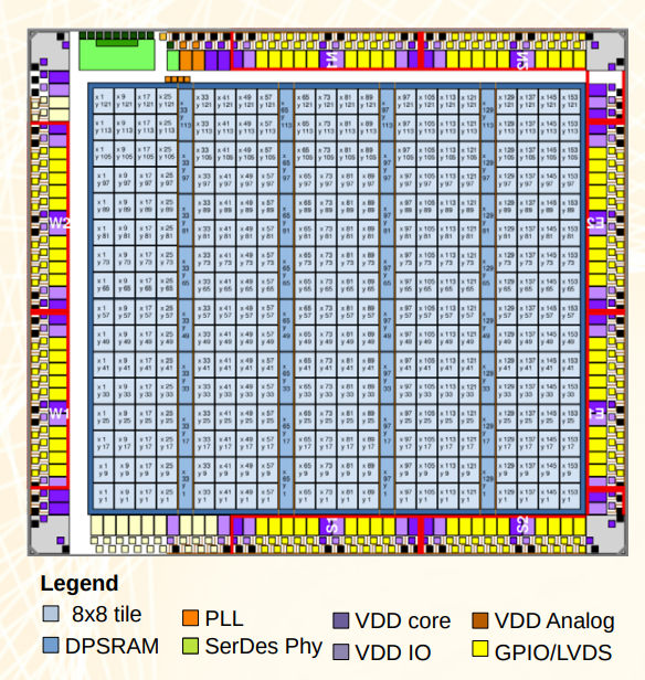
All this is based on a novel FPGA architecture combining CPE programmable elements with a smart routing engine. The CPE architecture allows an efficient building of arbitrarily-sized multipliers. Memory aware applications can use block RAMs with bit widths of 1 to 80 bits.
General Purpose IOs (GPIOs) can use different voltage levels from 1.2 to 2.5 Volt. All GPIOs can be configured as single-ended or LVDS differential pairs. Furthermore a high speed SerDes interface is available.
FPGA designs are synthesized using the Yosys framework. The free Cologne Chip P&R-software generates the FPGA bitstream.
A Static Timing Analysis (STA) is also performed and gives evidence about critical paths and the overall performance of a design. The design can be simulated using Verilog netlist and SDF timing extraction.
The devices are manufactured using GlobalfoundriesTM 28 nm SLP (Super Low Power) process. Due to manufacturing in Europe, there is no danger of trade restrictions or high taxation.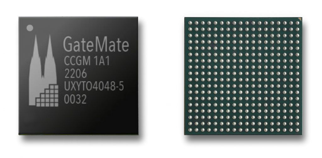
GateMate Features
Novel CPE Architecture
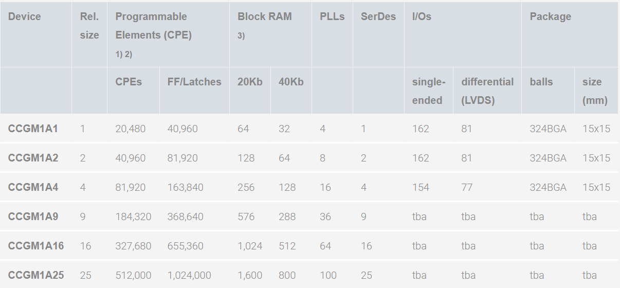
- 20,480 programmable elements (CPE) for combinatorial and sequential logic
- 40,960 Latches / Flip-Flops within programmable elements
- CPE consists of LUT-tree with 8 inputs
- Each CPE configurable as 2-bit full-adder or 2×2-bit multiplier
Low Power Consumption
- GlobalfoundriesTM 28 nm SLP (Super Low Power) process
- 3 operation modes: low power, economy, speed
- No excessive start-up currents
- Only two supply voltages needed, can be applied in any order
Features
- 4 programmable PLLs
- Fast configuration with quad SPI interface up to 100 MHz
- Multi-Chip configuration
- 1,280 Kbit dual ported block RAM with variable data widths in 32 x 40 Kbit RAM cells
- Multipliers with arbitrary size implementable in CPE array
- Multiple clocking schemas
- All 162 GPIOs configurable as single-ended or LVDS differential pairs
- Double data rate (DDR) support in all GPIO cells
- 2.5 Gb/s SerDes
Package
- 324-ball BGA package (15×15 mm)
- Only 2 signal layers required on PCB
GateMate(TM) Evaluation Board
The GateMateTM Evaluation Board is a feature-rich, ready-to-use development platform for the CCGM1A1.
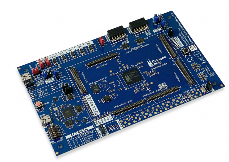
It serves as a reference design and for a direct entry into application development. User applications can be tailored to each of the six available I/O banks. Attaching additional hardware is a breeze thanks to the Pmod connectors: They allow access to a variety of peripheral boards, including motor controllers, sensors, displays and more.
• Six I/O banks + access to SPI/JTAG signals
• Two standard 12-pin PmodTM connectors
• 5 Gb/s SerDes via SMA connectors
• Access to all dedicated clock inputs
• Configuration via Flash on board, USB or JTAG
Memory:
• 64 Mbit Quad-I/O SPI Flash
• Up to two HyperBus memories on board (HyperRAM/HyperFlash)
Power:
• User-selectable core and I/O voltages
Ordering Information