Overview of Lookup Tables (LUT) in FPGA Design
17/04/2019, hardwarebee
Find electronic design, board design and module design companies:
Find FPGA design companies:
Find embedded software companies:
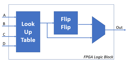
FPGAs are reconfigurable chips that are made up of individual logic blocks, each of which is composed of a flip flop and a Lookup Table (LUT).
You might have heard of the Lookup table (LUT) being referred to here and there and wondered what it does. if you are not familiar with the internal structure of an FPGA chip. Let’s take a brief but explanatory overview of the Lookup Table, or LUT, in an FPGA design.
What is a Lookup Table (LUT)?
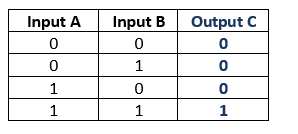
A Lookup Table, as the name suggests, is an actual table that generates an output based on the inputs. Here is an example for a lookup table that is implementing the function of an AND gate.

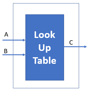
Try now to image that this table is stored in a small RAM. Inputs A and B are the address pins and C is the data pin. Every time your address pins are changing they are pointing at a different address entry and they are “reading out” the result which is 0 or 1 based on the inputs.

Lookup table is actually your customized truth table which is loaded with values that are relevant to your FPGA, based on your specific needs and instructions. You can even think of your custom Lookup Table or LUT as a small piece of RAM that is loaded whenever you power up your FPGA chip. It defines and directs the behavior of the combinatorial logic of your chip based on your VHDL or Verilog code, referring to the predetermined values to produce the desired results.
This means that the inputs you put into the Lookup Table are basically the address lines for a one bit wide RAM cell. As such, if you were to use a two inputs logic gate, it would make sense that it is able to produce or accommodate for four different combinatorial scenarios, thus making it suitable for a 4 x 1 bit RAM. You can keep increasing the number of inputs you wish to have and make subsequent modifications in the RAM you will be needing.
So, you can conclude, that Lookup Tables basically serve to act like logic gates in various combinations. Instead of having to connect a number of different NAND and NOR gates, you can simply use a Lookup Table to get all the possible combinations.
In an FPGA chip, the functionality is typically divided into a number of configurable logic blocks that are spread across the chip, each able to function independently and still produce coherent, singular results. Each logic block has its own set of flip flops as well as Lookup Tables. These Lookup Tables are what define the function of an FPGA and is the prime differing point between FPGA chips designed for various purposes. You should know that a table comprises of 1 bit memory cells that can hold either of two values: a 1 or a 0. Along with these memory cells are multiplexers. As discussed before, the number of inputs you need to feed into the table will be the prime determiner of the size of the device. The output values are called LUT-Mask and are made up of SRAM bits. After receiving the inputs, the device searches for the corresponding output value inside the SRAM block and produces it at the output pin.
Implementing Logic Functions with LUT
The logical function in various combinations is carried out by the chip using the Lookup Table. Any combinatorial logic function can be implemented in a lookup table. Lookup Tables in FPGAs help to significantly reduce the costs of computation and operation as it offers the computational range without requiring the time and massive gate count. Another one of the great advantages of using SRAM to store the information is that it offers the configurability feature which the FPGA chips are so well known and for. This means that the individual bits constituting the SRAM can be modified and reconfigured with every power up the chips goes through.
The Issue of Glitch in Lookup Tables
While the lookup tables in the FPGA chip designs offer much civics and use, there is one disadvantage that is often associated with them, and that is the glitch. A glitch is produced when there is an asynchronization between what the output is being shown as and what it should be due to the changing and rearranging of bits inside the SRAM of the Lookup table. As such, the block is uncertain of what the answer should be and produces a glitch which is basically an inaccurate output for a period of time. You may not even encounter such a problem with your use of the FPGA chip, but it is good to be aware of any problem that you may or may not encounter so you can be prepared in case it does arrive.
Advantages and Disadvantages of Lookup Tables
Advantages:
- Ability to implement any Boolean function
- Simplicity and ease of use
- Ability to be easily reconfigured
- Generally faster than programmable logic elements (PLEs)
Disadvantages:
- May require a large number of input variables and corresponding output values for certain functions, leading to impractical sizes
- May consume more resources within the FPGA compared to other implementation methods
- May have limited flexibility in terms of logical operations that can be performed compared to PLEs and other implementation methods
Lookup Table FAQ
Q: What is a lookup table in FPGA design?
A: A lookup table (LUT) is a digital circuit that can be used to implement any Boolean function in FPGA design. It consists of a series of input variables and a corresponding output value, which is determined by the input variables.
Q: How is a lookup table implemented in an FPGA?
A: A lookup table is typically implemented as a block of programmable logic within an FPGA. The input variables are connected to the FPGA’s programmable interconnect points, and the output value is generated by the LUT’s internal logic.
Q: Can a lookup table be used to implement any function?
A: In theory, a lookup table can be used to implement any Boolean function. However, the size of the lookup table may become impractical for certain functions, as it may require a large number of input variables and corresponding output values.
Q: How is a lookup table different from a programmable logic element (PLE)? A:
A programmable logic element (PLE) is a type of digital circuit that can be used to implement a Boolean function in an FPGA. A PLE consists of a small number of gates, such as AND, OR, and NOT gates, which can be configured to implement a specific function. A lookup table, on the other hand, consists of a series of input variables and corresponding output values, and does not use gates to implement the function.
Q: What are the advantages of using lookup tables in FPGA design?
A: Some advantages of using lookup tables in FPGA design include their ability to implement any Boolean function, their simplicity and ease of use, and their ability to be easily reconfigured. They are also generally faster than PLEs, as they do not require the use of gates to implement the function.

