
Clock Domain Crossing Techniques for FPGA
10/02/2020, hardwarebee
This document provides an overview of the importance of clock domain crossing (CDC) and introduces the reader to methods and techniques for taking care of clock domain crossing so that the design meets all functional requirements for a stable design. Improper clock domain crossing can cause the design to stop working at random times and hence can be disastrous if left unchecked.
This document is organized into the following sections:
- Background – Prepares the background required for further discussions
- CDC Synchronization Techniques – Discusses the synchronization techniques
FPGA Clock Domain Crossing (CDC) Background
This Section covers the following topics:
- Clock domain
- Meta-stability
A. FPGA Clock domain
A clock domain is a part of a design that has a clock that operates on a single clock and is often asynchronous to, or has a variable phase relationship with, another clock in the design. For example, a clock and its derived clock (via a BUFR, Divider) are in the same clock domain because they have a constant phase relationship. But, 100MHz and 59MHz clocks (whose phase relationship changes over time) are in two separate clock domains.
B. Meta-stability in FPGA
If a signal is passed between two clock domains then there is a chance that the signal could go meta stable, i.e a state where the signal is has not settled to either a high or low (1 or 0). In FPGA latching a meta-stable signal can cause entire designs to come to halt.
for example let us consider a case statement
case test-vector is
when ”000” = activate data-path 1
when ”011” = activate data-path 2
when ”001” = activate data-path 3
when others = do nothing
end case;
Here a meta-stable condition could cause the design to activate wrong data-paths or move the design to an invalid state.
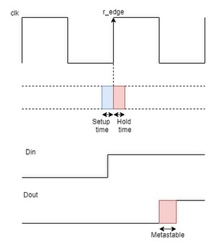
Fig. 1. meta-stability in FPGAs
Clock Domain Synchronization Techniques
Common methods for synchronizing data between clock domains are:
- Using m-FF based synchronizers.
- Using MUX based synchronizers.
- Using Handshake signals.
- Using FIFOs (First In First Out memories).
- Using Toggle synchronizers
- Using Xilinx specific clock domain crossing (CDC) tools
A. m-FF synchronizers
This Technique can be used if the following criteria is satisfied.
- the source clock domain is slower than destination clock domain.
- clock domain crossing (CDC) is on a control signal (either single bit or multibit).
By satisfying this criteria we can be sure that the destination clock captures any possible changes in signal without loss.
The idea here is that by keeping 2 FF in the destination clock domain, the signal has enough time for the meta-stability to settle down. This idea can be further extended to get m-FF synchronizers. Here the conditions to be satisfied is that Input Data of the m-flip-flop Synchronizer should be stable for at least m+1 clocks of the destination clock.
In Xilinx devices you can also add the attribute:
attribute ASYNC_REG : string;
attribute ASYNC_REG of destff1 : signal is ”TRUE”;
attribute ASYNC_REG of destff2 : signal is ”TRUE”;
This attribute places the destination flops as close as possible.

Fig. 2. 2-Flop Synchronizer
For multi bit clock domain crossing (CDC) using m-FF synchronizer, it is preferable to grey encode the control data. This is because, CDC only ensures that you are latching a stable signal at the destination clock domain, it does not ensure that you are latching the correct data. A grey encoded control signal has a hamming distance of one and hence any error due to CDC will keep the control in the previous state rather than moving to an illegal state
B. MUX based synchronizers
This technique is used when the following criteria is satisfied.
- The source clock domain is slower than destination clock domain.
- Clock domain crossing (CDC)is on a data bus.
- Data is stable for at least m+1 clock cycles.
Fig. 3. Mux Synchronizer
Clock domain crossing (CDC)on multiple bits using m-ff synchronizers can lead to data being skewed in time. This will lead the destination flops to register incorrect data. A mux synchronizer eliminates this problem by performing CDC on only a control signal which indicates to the destination clock domain that there is new data available on the bus. With this method we can be sure that the data that reaches the destination clock domain is stable and is not skewed in time.
We can extend the idea of MUX based synchronizers to get Handshake based synchronizers.
C. Handshake Signals
This technique is used when the following criteria is satisfied.
- source clock domain is slower than destination clock domain.
- clock domain crossing (CDC) is on a data bus.
- Data is stable for at least m+1 clock cycles.
Handshake signals is just an extension of mux based synchronization with an additional acknowledgment line.

Fig. 4. Handshake
The functionality is as follows:
The source clock latches updated data onto the source FF, then raise a request command to the destination clock. the request signal is passed through an m-ff synchronizer to the destination clock domain. The destination clock domain latches the data as soon as the request signal is received and sends an acknowledgment signal back to the source clock domain.The source clock domain updated the data in the bus as soon as the acknowledgment signal is received.
Using handshake signals eliminates the problem caused by toggling data. This ensures higher data integrity over CDC.
D. Dual clock FIFO synchronizers
Clock domain crossing (CDC) on multiple bits, either data bits or control bits, can be done through using ”Dual clock FIFO synchronizers” . A ”Dual clock FIFO synchronizer” is a register buffer where data is inserted from the write clock domain and data is removed from the read clock domain. Since both work within their own respective clock domains, using a dual-port buffer, such as a FIFO, is a safe way to pass multi-bit values between clock domains.
A ”Dual clock FIFO synchronizer” uses a write pointer working in the write clock domain using a grey counter and a read pointer working in the read clock domain using another grey counter. Using a grey counter for read and write pointers assures accurate functionality.
In Xilinx devices, we can use inbuilt fifo IP’s integrated with either vivado design suite or ise. Another option is to use the following primitives.
E. Toggle synchronizer
This technique is used when the following criteria is satisfied.
- source clock domain is faster than destination clock domain.
- Clock domain crossing (CDC)is on a single bit.
Toggle synchronizer is used to synchronize a pulse generated in a faster clock domain to a slower clock domain. In such scenarios a m-ff synchronizer fails as the destination ff may skip the incoming data pulse. The diagram below shows the implementation of a toggle synchronizer.
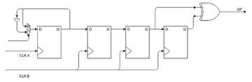
Fig. 5. Toggle synchronizer
The functionality is as follows:
A pulse in FF1 will create a continuous high/low signal in FF2 which is then delayed and passed through a rising/falling edge detector in the destination clock domain to recreate the pulse.
F. Xilinx (AMD) Specific Clock Domain Crossing (CDC)Tools
In Xilinx devices, there are inbuilt primitives which can be used for taking care of CDC’s. These are the XPM CDC primitives which can be accessed from the language templates.
They include:
- Asynchronous Reset Synchronizer
- Bus Synchronizer with Full Handshake configurations
- Pulse Transfer • Single-bit Array Synchronizer
- Single-bit Synchronizer
- Synchronizer via Gray Encoding
- Synchronous Reset Synchronizer
Details on each of these synchronizers can be obtained from the Xilinx documentation.