
Step by Step Guide: Analog Design
04/05/2021, hardwarebee
Analog design is one of the most critical blocks in any electronic project. It is the fundamental connection between an idea and the real world. In many cases, even well-conceived schematics and high-quality components fail to achieve their required performance if the analog blocks are poorly designed. Therefore, the objective of this analog design article is to provide a step-by-step guide and useful insights to help you achieve the best performance from your analog circuit design.
Analog Design Components
The main building blocks of any analog circuit design are the electrical components. They can be divided into two categories: active components and passive components. Active components are the blocks powered by a voltage supply, capable of controlling or modifying electrical signals, and are represented here by the transistors and the operational amplifiers. Passive components, on the other hand, do not require power supplies to operate. The most fundamental passive components are the resistor, the capacitor, the inductor, and the diode.
- Resistor: is a passive component that converts electrical current to electrical voltage (or vice-versa), while dissipating power in the process. Resistors can be used for current limiting, signal conditioning, cut-off frequency selection in filters, gain control in amplifiers, heating devices, etc. Resistors are characterized by two factors: material and tolerance. The right material depends on the application and desired cost of the circuit, with metal-film resistors having the best cost-benefit, thick-film resistors providing low parasitic effects and surface mount resistors are used for space limited boards. Also, special types of resistors can offer some specific capabilities, such as variable resistors, thermistors, and light-dependent resistors, which can be used as sensors.
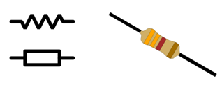
Figure 1: Resistor symbols and package
- Capacitor: is a passive component capable of storing electrical energy between two metal plates and a dielectric insulator. This property defines a constant ratio between charge and voltage. In analog circuits, capacitors are used with two main objectives: to modify the dynamics of the electric signal, and to provide a local access to energy. The first is widely applied in filters, signal conditioning, oscillators, and control systems; whereas the second is needed when the power supply is too far away from the circuit, providing a low resistance path to energy. Capacitors are also classified by their material, with ceramic and film capacitors being used for applications that require lower values of capacitance, and electrolytic capacitors being used for low frequency and large energy storage.
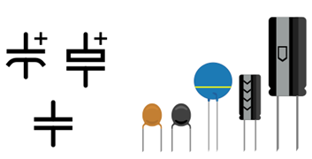
Figure 2: Capacitor symbols and packages
- Inductor: Inductors are components that store magnetic energy. They are composed by copper wires in the shape of a coil, a core, and a package for encapsulation. Because of its magnetic properties, inductors provide a constant relation between voltage and the derivative of current. Therefore, inductors are widely applied to modify the dynamics of a signal, being used in control systems and high-quality resonant filters.
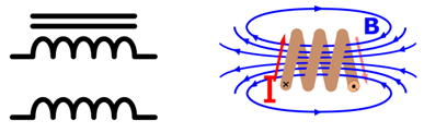
Figure 3: Inductor symbol and the magnetic energy storage mechanism
Inductors can also be used in series with the power supply, to prevent high frequency surges of current, reducing the overall noise of the system. Its energy storage capabilities are fundamental to switched-mode power supplies. They can be classified by the core material and shape. The core material can be air, ferrite (high frequency applications) and iron (high inductance values, but limited application range). Inductors come in various shapes: round, square, toroidal. The shape defines the effective size of the inductor, and influences some parasitic parameters, such as energy loss.
- Diode: is a passive non-linear component. Diodes are typically made using a PN junction, although some diode types are made using a metal-semiconductor junction, such as the Schottky diode. Diodes allow current flow in only one direction. The most fundamental diode application is the rectifier, which converts AC current to DC current. Diodes are also applied in signal conditioning, switched-mode power supplies, heaters, sensors, and voltage regulators. Diodes are usually categorized by their voltage and current rates. Besides normal diodes, special diodes are also available, such as the Schottky diode (used in fast switching applications), Zener diodes (for voltage regulation) and light-emitting diodes (LED).
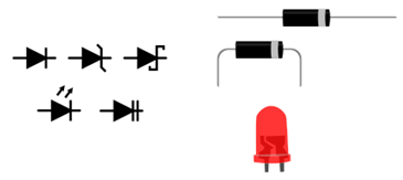
Figure 4: Diode symbol and packages
- Transistor: The transistor is the fundamental active block of any electronic circuit, and it can be applied both in analog and digital applications. The transistor works by controlling the amount of current passing between two terminals using a signal (voltage or current) applied to a third terminal. Three main types of transistors are typically available: bipolar junction transistors (BJT), metal-oxide-silicon field transistors (MOSFET) and junction field transistor (JFET). Each type differs in terms of operation mechanism, but in practical terms: a BJT provides a current controlled by current and a MOSFET or a JFET provides current controlled by voltage.
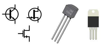
Figure 5: Transistor symbol and packages
Any type of transistor can be applied as an amplifier, a switch, or a voltage-controlled resistor, but some are more fitted to specific applications. BJTs are widely applied in audio amplifiers, MOSFETs are used in switching-mode power supplies, and JFETs are often applied as voltage-controlled resistors.
- Operational Amplifier: Operational amplifiers (OPAMPs) are active components made of integrated transistors and passive components. This device subtracts two input voltages and multiplies the result by a high gain. The open loop gain of the OPAMP is typically very high and non-linear, requiring negative feedback to be useful in analog applications. The nature of the feedback network usually defines the operation performed by the OPAMP: a resistive feedback results in a linear signal amplifier, a capacitive or inductive feedback results in an active filter or resonance oscillator and a transistorized feedback can be used to perform complex operations, such as logarithm, anti-logarithm and multiplication.
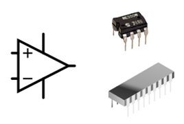
Figure 6: Op Amps symbol and packages
There are many types of amplifiers based in OPAMPs in the market: current-feedback amplifiers, instrumentation amplifiers (INA), high-frequency amplifiers, transconductance amplifiers (OTA), etc. The designer should select one based on the application requirements: for instance, INAs are used to amplify differential voltages while rejecting common-mode signals, and OTAs can be used as voltage-controlled current sources.
Analog Design Tools
During the early days of analog circuit design, circuits were developed using hand-made schematics and calculations, without the possibility of simulating before testing. Nowadays, the hardware designer can rely on several digital tools to conduct a project. Schematic CAD (Computer Aided Design) tools can be used to design schematics from scratch. Simulation programs can then be used to predict the circuit outcome before testing, calculating the signal behavior both in time and frequency. Some popular simulation tools in the market are the PSpice, LTSpice, Tina-TI and Multisim.
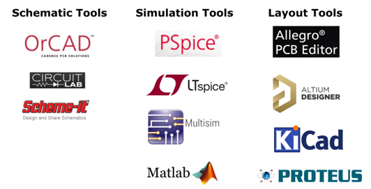
Figure 7: Automatic design tools used for schematic, simulation, and PCB layout
Analog circuit simulation is a powerful tool that allows the designer to further tune the component values of a schematic before needing to design the layout, which reduces engineering time and work. Finally, layout tools are used to design the printed circuit board (PCB), where the designer can define the component distribution, the routing paths, the number of layers, the vias, the paths, etc. Popular layout tools are Allegro, Altium, Eagle and KiCAD. The combination between the schematic, simulation and layout software should be selected wisely, to optimize the design flow. Cost should also be considered, as many design tools are considerably expensive for the average consumer.
Analog Design Example: Low-Pass Filter
Schematics
The first step of any analog design is the electronic schematic. This is the fundamental drawing that will describe your project in terms of electrical diagrams. To begin the concept of any schematic, you need the design specifications. The requirements vary greatly from project to project, but they should always be the starting point. In our example, we define the following design specifications:
- Functionality: Low-Pass Filter
- Gain: 40 dB
- Cut-Off frequency: 1 kHz
- Rejection Band: < 100 kHz
- Gain at the Rejection band: -40 dB
- Ripple: 0 dB
Now that we have our specifications, we can define the topology. From the cut-off frequency and rejection band information, we can establish the transition band of the filter, which is 2 decades (1 kHz to 100 kHz). These values combined with the gain information gives us the order of the filter to be used, which is 2 (40 dB/decade). Filters can be found in many topologies, so for design purposes we can specify another rule:
- The analog circuit should be designed with the minimum number of active components possible: This optimizes the overall cost, as well as reducing the parasitic effects intrinsic from the active circuits. However, this is not a general rule.
From the literature we know that second-order active filters can be implemented using the multiple-feedback topology, which requires only one OPAMP and several passive components (Figure 8). Now we need to define the OPAMP model and the value of the passive components.
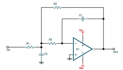
Figure 8: Multiple-Feedback Filter Topology
To select the component values, one should use the mathematical model of the circuit to meet the specifications provided. Besides frequency and gain, we also established the amount of ripple of the filter. Using this information, one can apply the model equations to figure out the component values. However, this process can be very onerous for complex systems, due to the number of variables and the non-linearity of the equations. Fortunately, for popular circuits, several automatic design tools are available. For instance, the Webench Filter Design Tool, from Texas Instruments™, can output an entire filter design based on the specifications. Using our project requirements, the circuit showed in Figure 9 was generated, as well as a bill of material (BOM) list containing each component value and tolerance.
Other automatic design tools are available in the market, with but the reader should keep in mind that they are meant to popular circuits, such as filters, oscillators, and switched-mode power supplies. Novel circuits require solving the model equations manually. In these cases, symbolic solving programs, such as Maple and Maxima, are extremely useful, as they can automatically reduce the equation systems to more treatable forms.
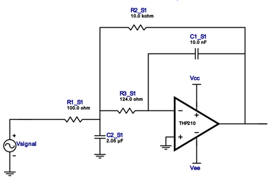
Figure 9: Filter designed using the Webench Filter Design Tool, from Texas Instruments™
Analog Design Simulation
Simulation is an important step of electronic design, although it is sometimes neglected by engineers. Using simulations, one can tune the component values, adjusting them to achieve optimum performance. Also, different component models can be tested without needing to recalculate the model equations. For example, let consider that we do not have access to a THP210 amplifier, but we have one AD825 (from Analog Devices™) spare in the laboratory. To verify if the AD825 is still able to achieve the filtering properties that we need, we can run a simulation in PSPICE to validate the frequency behavior of the new filter.
Using ORCAD Capture, we draw the schematic using the AD825. We feed the circuit with a ±10 V voltage supply. Figure 10 shows the new schematic, as well as the main functionalities of the environment: Schematic Tools, Simulation Tools, Component Selection and File Hierarchy.
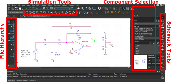
Figure 10: Simulated schematic and the ORCAD Capture Environment
The first simulation performed is an AC Sweep, which verifies the frequency behavior of the filter. From Figure 11, one can see that the frequency response is similar to the one obtained by the Webench Filter Design tool, proving that changing the amplifier did not modified significantly the filter behavior. Besides AC sweep, PSPICE and other simulators provide transient simulation, BIAS point calculation, DC Sweep, noise analysis, Monte Carlo simulations, etc. In our case, the Monte Carlo simulation is important to check the envelope of the gain curve, that is, if the variations caused by component tolerances are acceptable. The Monte Carlo simulation was performed using 100 runs and a Gaussian distribution of component values, resulting in a worst-case variation smaller than 1.0 dB. This variation in the gain is acceptable, considering the design specifications of our project.
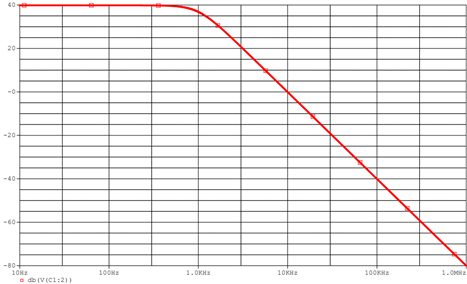
Figure 11: Filter gain (in dB) as function of frequency
Circuit Layout
After the analog design is complete and validated by simulations, the engineer must design the printed circuit board (PCB). Many designers tend to neglect the negative effects caused by poor routing, but this is not the most efficient approach. When developing an electronic project, one should treat the PCB as a crucial component of the circuit, that must be designed carefully to avoid practical problems.
The first step is to select the PCB editor. There are many options in the market (as seen in Figure 7), and often schematic/simulation tools can be interfaced with the PCB editor, allowing to simply export the NETLIST from one TO the other. For instance, PSPICE schematics can be automatically exported to Allegro. However, for didactic purposes, we will use the KiCAD™ software.
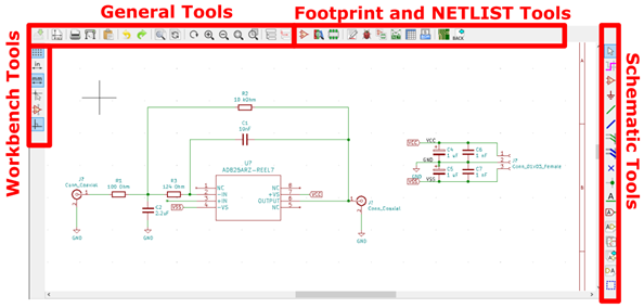
Figure 12: Filter schematic transcribed to the KiCAD software
Figure 12 shows the same schematic from Figure 9 in the KiCAD™ schematic editor. Components that are not already in the KiCAD™ library, such as the AD825 operational amplifier, can be downloaded from the internet. One useful website is the UltraLibrarian™, which is a PCB CAD Library containing footprints and symbols compatible with most PCB editors, including KiCAD™. After drawing the schematic, each component symbol must be associated with a footprint. Finally, the netlist should be exported to the PCB editor.
Now the routing really begins. First, the designer must define the design rules, that is: number of layers, via size, minimum path width, minimum distance between components, etc. These parameters are dependent on the fabrication method and the circuit requirements. After that, the outline of the board must be defined, and the components should be distributed inside. Then, the designer should draw the paths of each net of the circuit. Auto-routing is a powerful tool, that should be applied carefully in complex designs. However, in our case, it is easier to draw the paths manually.
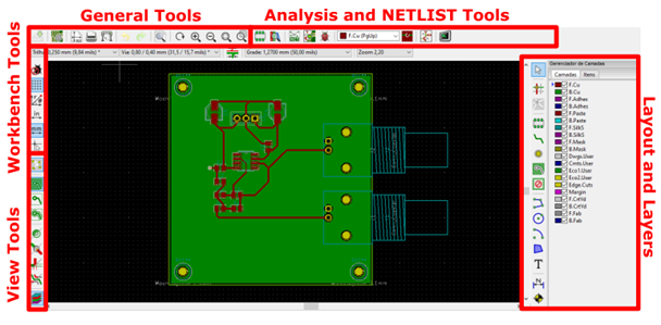
Figure 13: Layout of the filter and the KiCAD™ PCB Editor environment.
Tips & Tricks for PCB Design
- Decoupling Capacitors: note that we added four capacitors to the original schematic, directly connecting them to the supply. This provides local current supply for the circuit, which reduces voltage drops and high frequency noise. The larger electrolytic capacitors supply AC currents for the whole circuit, and the smaller ceramic capacitors should be placed near each active component to provide high frequency currents.
- Ground Planes: the lowest impedance paths for ground currents are dependent on the frequency. That is why a ground plane is always recommended. The ground plane provides freedom to the ground currents to follow the paths of lowest impedance, avoiding ground loops. Also, the plane provides shielding from external noise.
- Power Planes: for the same reason ground planes are necessary, power planes are recommended for circuits with several active components and power connections. This approach reduces supply noise and losses.
- Digital vs Analog Circuits: digital circuits produce high frequency spikes that can significantly degrade the analog circuits. For mixed-signal circuits, one should separate analog from digital stages. Guard rings should also be placed around the analog stage for extra protection.
- Path Loops: avoid forming loops when routing the paths, specially if they are signal paths. Path loops generate parasitic inductance and antennas, which irradiate energy and can couple noise from external sources.
- Differential signals: when using differential signals, the routing of the pairs should be done equally: each path should be identical to the other, to avoid impedance and coupling mismatches.
After finishing the layout, one should run a DRC error analysis. This tool searches for violations of the design rules, as well as mismatches between the NETLIST and layout. Finally, using the 3D viewer tool, one can verify the final appearance of the PCB, and check if the component spacing is feasible. Figure 14 shows the 3D view of our example.
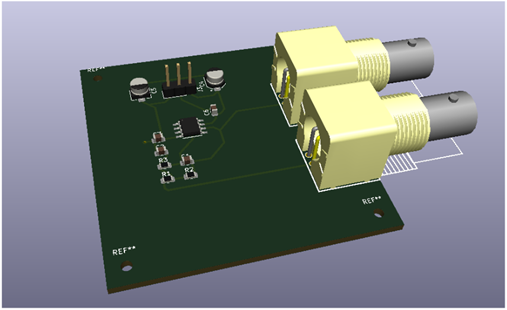
Figure 14: 3D view of the printed-circuit board designed
Now, we can finally export the Gerber files and send them to the manufacturer, that will print the PCB. After that, the designer should weld the components and test the board to validate its performance. The whole design flow is an iterative process: if everything runs properly, the design flow ends; if not, the designer should return to the previous steps and correct the problem.


