Top 10 PCB Layout Tips for Beginners
01/04/2020, hardwarebee
Printed Circuit Board Design is a skill that will help you in making your own electronic product whether as a professional or as a hobbyist. In the professional world of electronics engineering, one can find PCB in any electronic device, such as: mobile phone charger, toys, washing machines etc.
In this article, you will able to learn how to design your own professional PCB board’s (including schematic, PCB layout, gerber generation & 3D Model). We will provide you best tips and tricks including free software’s that will help you to polish your skills from beginners to expert level in PCB layout design & electronics field.
We will cover the following topics:
- Top 10 PCB design software’s in 2020
- Components Footprint Selection & Arrangements
- Top 10 Routing Tips for PCB layout
- Six Basic Design Rules for Any PCB Design
- Single Vs Multilayer PCB design
- PCB shape and size
- SMT vs Through Hole
- Generating Gerber Files
- 3D View of project /CPL files
- Design Smart Watch PCB
Top 10 PCB Design Software
Here are top 10 professional PCB design software’s that can be used to design any type of printed circuit board. Some of these softwares are free to download and use.
- Altium Designer
- Autodesk EAGLE
- KICAD EDA
- Easy EDA online
- Diptrace
- SolidWorks PCB
- Express PCB Plus
- OrCAD Capture
- Circuit Maker
- Multisim Ultiboard
Components Footprint Selection
After designing the schematic or circuit diagram using one of these above mentioned software. You’ll need to test the ERC (Electrical Rules Checking), it will help you to verify joints and connection in designed schematic.
After a successful ERC test, the next step is to select the right footprint for the PCB board. After selecting the right footprint for your components, the next step is to arrange, rotate each component at specific location. When you are arranging components, keep practical board in mind, which you want to see as a final product.
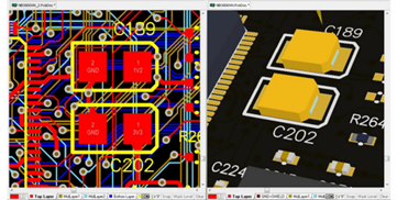
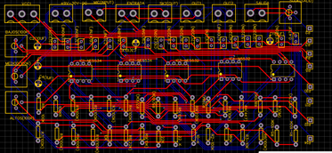
Top 10 PCB Design Routing Tips
In electronic design, wire routing, commonly called simply ‘routing’, is a step in the design of printed circuit boards (PCBs). It builds on a preceding step, called placement, which determines the location of each active element of an IC or component on a PCB. Here are top 10 PCB design routing steps:
- Always Create a Ground Plane
- Use Vias to Remove Heat
- Don’t Rely on Your Auto router – make sure you check critical nets with your own eyes
- Understand Your Manufacturer’s Specifications – follow the layout suggestion of each vendor
- Figure Out Your Trace Widths – talk to your PCB manufacturer to get their design rules
- Leave Enough Space Between Traces – talk to your PCB manufacturer to get their design rules
- Make Your Job Easier with the Snap Grid
- Avoid Using 90 Degree Trace Angles
- Leave Room Between Traces and Mounting Holes
- Make Your Power and Ground Traces Wider
6 Basic Design Rules for Any PCB Design
All of our PCB designs have a logical and physical side that need to be properly managed in order to create the perfect design so what do design rules do.
They allow you to define a system so you can automate the checking of these requirements and giving you an interface between the logical and physical side. When you actually have these rules to define these requirements, you’re will able to automate DFM checks and make sure that you have a board that can be manufactured.
- Polygon Connect Style
- Solder Mask expansion
- Routing Via style
- Component Clearance
- Electrical Clearance
- Routing Width
Single Vs Multilayer PCB design
Double sided PCB and single sided PCB are essentially the same. The difference being is that a single sided board has copper on one side of the board. Technically speaking, a single-sided board will not have copper plated in the drilled holes either. A multilayer PCB has more than two layers
SMT Vs Through hole
Through-hole mounting is the process by which component leads are placed into drilled holes on a bare PCB. Whereas SMT components are secured only by solder on the surface of the board, through-hole component leads run through the board, allowing the components to withstand more environmental stress.
PCB Shape and Size
It’s not uncommon to see round, triangular, or other interesting PCB shapes. Most PCBs are designed to be as small as possible, but that’s not necessary if your application doesn’t require it.
If you plan on putting the PCB into an enclosure, the dimensions may be limited by the size of the housing. In that case, you’ll need to know the enclosure’s dimensions before laying out the PCB so that everything fits inside.
The components you use will also have an effect on the size of the finished PCB. For instance, surface mounted components are small and have a low profile, so you’ll be able to make the PCB smaller. Through hole components are larger, but they’re often easier to find and easier to solder.
Generating Gerber Files
The Gerber format is an open 2D binary vector image file format. It is the standard file used by printed circuit board (PCB) industry software to describe the printed circuit board images. Gerber files are necessary to manufacture and assembly the final PCB boards. It contains:
- Bottom Copper (GBL)
- Bottom Silkscreen (GBO)
- Bottom Solder mask (GBS)
- Top Copper(GTL)
- Top Silkscreen(GTO)
- Top Solder mask (GTS)
- Drill file (TXT)
- Drill station Info File(dri)
- Photo plotter info file (gpi)
- Mill Layer (GML)
- Top Paste (GTP)
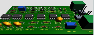
3D View of project
Electronics projects looks amazing in 3D view. We can see the final PCB design in Top, bottom, left side, right side, at specific angles. Here are some samples PCB boards in 3D.