HardwareBee
https://www.nuvation.com/
  • Find ASIC Vendors
  • Design Services Directory
    • FPGA Design Services
    • Electronic Design Services
    • Embedded Software Companies
    • Add your company
  • Get Price Quotes From Vendors
    • Electronic Design Companies
    • FPGA Design Companies
    • Embedded Software Companies
    • Design & Manufacturing Companies
    • Get IC Device Prices
  • Emerging ICs Directory
    • UWB
      • Spark Microsystems
    • FPGA
      • Colonge Chip
      • Rapid Silicon
    • Radar
      • Acconeer
    • Add your IC
  • Get IC Prices
  • WikiBee
  • Resources
    • FPGA Academy
    • Embedded Academy
    • FPGA vs ASIC Calculator
    • Watt to dBm Converter
    • dBm to Watt Converter
  • Pricing
    • Get Your Company Listed
    • Book a Demo
    • Get a Monthly Lead List
HardwareBee
  • Design Services Directory
    • FPGA Design Services
    • Electronic Design Services
    • Embedded Software Companies
    • Add your company
  • Get Price Quotes From Vendors
    • Electronic Design Companies
    • FPGA Design Companies
    • Embedded Software Companies
    • Design & Manufacturing Companies
    • Get IC Device Prices
  • Emerging ICs Directory
    • UWB
      • Spark Microsystems
    • FPGA
      • Colonge Chip
      • Rapid Silicon
    • Radar
      • Acconeer
    • Add your IC
  • Get IC Prices
  • WikiBee
  • Resources
    • FPGA Academy
    • Embedded Academy
    • FPGA vs ASIC Calculator
    • Watt to dBm Converter
    • dBm to Watt Converter
  • Pricing
    • Get Your Company Listed
    • Book a Demo
    • Get a Monthly Lead List
5443 Views

Introduction to SPI Interface and Protocol

29/12/2019, hardwarebee

Get a Price Quote

SPI stands for Serial Peripheral Interface. Developed by Motorola in the 1980s, SPI protocol is now a specification standard for short distance communication especially in embedded systems.


How Does SPI Protocol Work?


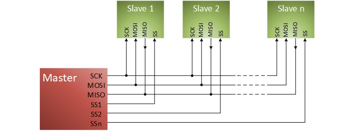
The SPI architecture is a typical master slave structure having a single master and communicating with the connected devices in full duplex. The master device is what gives the frame for reading and writing purposes whereas the slave devices are supported with the help of the slave select or the chip select lines. In the case that only one slave device is being used, it is possible to attach the slave select pin to the logic low if permitted by the slave. In the case that multiple slave devices are being used, each slave device will require an independent slave select signal from the master device in order to operate.


The master starts with selecting the slave device that is the target for the data transfer (either read or write cycles). The clock cycle is then issued, only after the master device has waited out any time that may be required for tasks such as analog to digital conversion. Apart from setting the clock frequency, the master device is also responsible for setting the clock polarity (CPOL) and phase (CPHA). During the data transmission process, the master sends a bit of data on the MOSI line which is the Master Output Slave Input or Master Out Slave In line (meaning the master device is giving the output of data) and reads it as well. If a certain slave device does not receive an activation signal on its chip select line, the input clock must be ignored by that slave and it should not respond to the MISO signal. Sometimes, there may be a need to implement an external tristate buffer to ensure this.


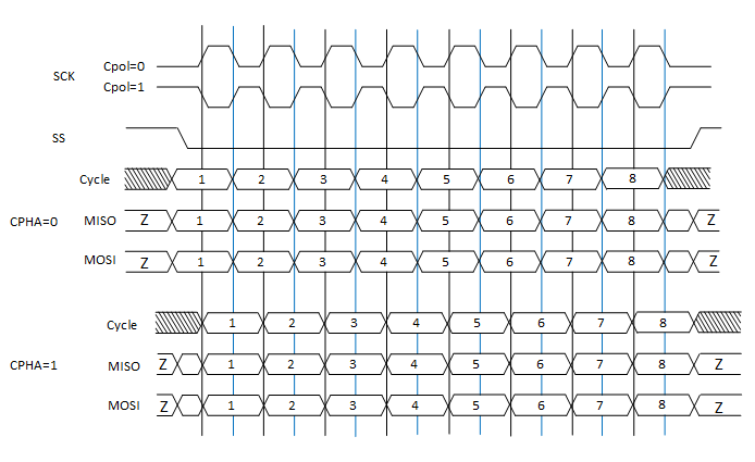
Two shift registers are involved in the data transmission process, one each placed with the master and the slave device respectively. Register bits are continually shifted out and in until the master and the slave device have essentially exchanged the register values since the registers are connected in a virtual ring topology. In the case that more data needs to be transmitted and the cycles need to continue, the shift registers return to their original values or locations and the process repeats once again or however many times as needed for the complete transmission of the intended data. Typically, eight-bit words are used for the transmission of data in an SPI but variations have been observed in the word size with digital to analog and analog to digital converter using twelve bit word sizes, and touch screen controlling devices and audio codecs using sixteen bit word sizes.


Slave vs. Daisy Chain Configuration in SPI


Conventionally, SPI is used in an independent slave configuration but some applications require the use of the daisy chain configuration. In the independent slave configuration, an independent chip or slave select line is present for each of the slave devices. This means that the master is only able to control or activate one slave at any given time. In a daisy chain configuration, on the other hand, the first slave output is connected to the second slave output and the chain continues on with the number of slaves attached to the master in the system. This means that when the second pulse of clock signals goes out, each of the SPI ports also sends along a copy of the first clock signals as well. This essentially creates a communication shift register.


SPI Applications


SPIs are frequently used in embedded systems for examples:  Secure Digital cards, LCDs interface, A2D or D2A interfaces. They are used in embedded systems since they give great savings. They are used across a variety of different applications such as in FLASH and EEPROM memories, real time clocks, communications chips such as Ethernet and USB, audio codecs, SD cards, and a number of different kinds of sensors such as temperature and pressure, among others.


SPI Advantages


There are a number of features that make SPI the best choice for many applications.


  • SPI has great signal integrity and operates at high speeds thanks to the push pull drivers instead of the conventional open drain system.
  • In terms of the data transfer, there is a lot of freedom and flexibility in terms of bits transferred and message specifications.
  • The hardware normally does not take up too much power because of less circuitry, no failure modes are associated with it, there is no need for precision oscillators since the slaves use the clock of the master, and there is no need for transceivers either.
  • The default version of the protocol uses full duplex mode communication.
  • Unidirectional signals.
  • Only four pins on the IC packages are used.


SPI Disadvantages


Unfortunately, it is not all paradise in the world of SPI and there are still a number of issues that need to be addressed.


  • Needs even more pins as compared to I2C.
  • The slave is unable to give any hardware flow control.
  • There is no acknowledgement of the hardware of the slave device, meaning its loss is not detected by the master.
  • In the case of a shred bus, you would need out of band chip select signals since there is no in band addressing.
  • There is no currently described error checking protocol making the process error prone.
  • Is limited to handling extremely short distances only, especially when compared to some of the other standards such as RS-232 or CAN-bus.
linked in icon
Sign up for HardwareBee
* = required field

Recent Stories

What is a Piezo Driver IC and how to Choose one
Introduction to Hall Effect Sensor ICs
The Ultimate Guide to: Oscillator ICs
Low Noise Amplifier: Ultimate Guide
ASIC Prototyping
FPGA Prototyping Services
QFN Socket
QFN Socket
FPGA in Medical and Healthcare
Get 3 Quotes from Electronic Design Companies
Get 3 Quotes from FPGA Design Companies
Get 3 Quotes from Embedded SW Services
Get 3 Quotes from EMS Companies

Find Design Services

Get IC Prices

Get Price Offers From
  • Electronic Design Services
  • FPGA Design Services
  • Embedded Software Companies
  • PCB Layout Services
  • Printed Circuit Board Manufacturers
  • Design & Manufacturing Services
Welcome New Vendors
  • Spark Product Innovation
  • QBayLogic
  • Fidus Systems
  • nao.design
  • HQ NextPCB
Browse Vendor Directories
  • Electronic Design Companies
  • FPGA Design Companies
  • Embedded Software Services
  • Manufacturing Companies
Featured Vendor

Micro Technology Services

Recent Posts
  • What is a Piezo Driver IC and how to Choose one
  • Introduction to Hall Effect Sensor ICs
  • The Ultimate Guide to: Oscillator ICs
  • Low Noise Amplifier: Ultimate Guide
  • ASIC Prototyping
Most Popular Blog Posts
  • The Ultimate Guide to: Variable Gain Amplifier
  • FPGA for AI (Artificial Intelligence): Ultimate Guide
  • PCB Stackup: Ultimate Guide and Examples
  • The Ultimate Guide to Logic Chips
  • FPGA Video Processing: Ultimate Guide

Never miss an update!

Follow us on LinkedIn

Do you need any price
information?

(Electronic design, FPGA design, Embedded SW services, PCB design, Turnkey)

Yes
No
This page is sponsored by
HardwareBee

Copyright 2017-2024, HardwareBee. All rights reserved.

  • About Us
  • Contact
  • Subscribe
  • News
  • Get Free Support
  • Get listed
  • Send a wiki/article
  • Advertise

Follow Us

Be sure to follow our LinkedIn company page where we share our latest updates LinkedIn
Partner with us Partner with us

Design and Manufacturing Services

  • Engineering Design Services
  • Electronic Design and Manufacturing
  • Electronic Product Development
  • Electronic Product Design
  • Electronic Consulting Services
  • Electronic Engineering Companies
  • Electronic Engineering Services
  • Electronic Product Design and Development
  • Electronics Design Services
  • Electronics Design Company
  • Electronic Design Consultants
  • Electronic Design Company
  • FPGA Design Company
  • FPGA Consultant
  • FPGA Design Services UK
  • Electronics Manufacturing services
  • Electronics Manufacturing Companies
  • Electronic Contract Manufacturing Companies
  • Electronic Manufacturing Services Companies
  • EMS Companies Directory
  • Electronic Design Services
  • FPGA Design Services
  • Embedded Software Companies
  • PCB Layout Services
  • Printed Circuit Board Manufacturers
  • Design and Manufacturing Services
X

Don’t miss anything, follow us on LinkedIn

https://www.linkedin.com/company/hardwarebee/

We are using cookies to give you the best experience on our website.

You can find out more about which cookies we are using or switch them off in .

Privacy Overview

This website uses cookies so that we can provide you with the best user experience possible. Cookie information is stored in your browser and performs functions such as recognising you when you return to our website and helping our team to understand which sections of the website you find most interesting and useful.

Strictly Necessary Cookies

Strictly Necessary Cookie should be enabled at all times so that we can save your preferences for cookie settings.

If you disable this cookie, we will not be able to save your preferences. This means that every time you visit this website you will need to enable or disable cookies again.

3rd Party Cookies

This website uses Google Analytics to collect anonymous information such as the number of visitors to the site, and the most popular pages.

Keeping this cookie enabled helps us to improve our website.

Please enable Strictly Necessary Cookies first so that we can save your preferences!

Additional Cookies

This website uses the following additional cookies:

(List the cookies that you are using on the website here.)

Please enable Strictly Necessary Cookies first so that we can save your preferences!