FPGA Projects and (free) Source Code
03/02/2021, hardwarebee
Find electronic design, board design and module design companies:
Find FPGA design companies:
Find embedded software companies:
This article covers FPGA projects from beginners to expert level. You can find here FPGA projects for engineering students, cool FPGA projects and FPGA projects used in commercial products. All FPGA projects are with free and downloadable source code, allowing you to use the projects at home or at work. Our goal is to help users understand FPGA’s role in the industry and how FPGAs are used to implement various functions in an electronic products.
Frequency Hopped Radio on FPGA
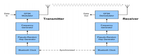
The first FPGA project on the list is a standard spread spectrum system is of the “direct sequence” or “frequency hopping” type, or else some combination of these two “hybrids”. In frequency Hopping, the system” hops” from frequency to frequency over a wide band. The pattern in which frequencies are engaged is a role of a code sequence, and the rate of hopping from one frequency to another frequency is a function of the data rate.
This FPGA project aims to design, simulate and develop a transmitter and a receiver for frequency hopped system on FPGA using VHDL. This project’s completion covers the art of secure digital communications that is now being exploited for commercial, industrial and military purposes.
The transmitter design includes the following blocks; PN sequence block; serial to parallel converter; random input block; frequency synthesizer; mixer block.
Click here to download the FPGA source code

Figure 1: Frequency Hopped Radio Architecture
Digital Video Scalar on FPGA
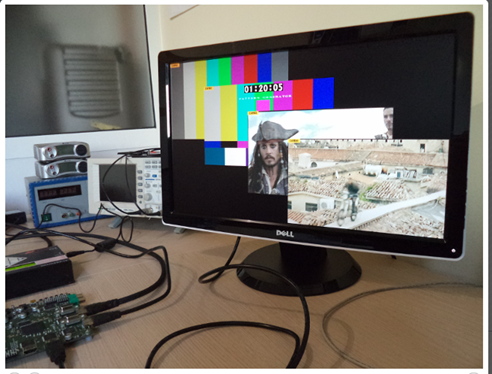
Digital video up/down scaler accepts RGB or YCbCr 444 video and permits independent horizontal and vertical scaling to generate any desired resolution or aspect ratio. Uses a 7×7 FIR polyphase filter with 18 phases to generate a high-quality video output. Supports 2K video and above. There is no need to do the frame buffering. This video streamer scales streaming video up and down in resolution. I used the Bilinear, and nearest neighbour resizes modes. The code provides the input and output resolution, scaling factor and scaling as well.
Click here to download the FPGA source code

Figure 2: Video Scalar
Canny Edge Detector on FPGA
Canny edge detection is a multi-stage algorithm for vision processing that generates a binary output image (edge or no edge for complex vision algorithms such as number plate identification). Detection of Canny edges can eliminate irrelevant image information and provide a clear binary output for each pixel. High-performance computing is traditionally implemented by Canny edge detection. However, you can now implement vision algorithms for low-power mobile applications on embedded platforms. Multiple processing stages include vision algorithms such as Canny. Usually, processors have to fetch, process, and write the input image frame from external memory back to external memory. For the next processing block, the processor repeats this process. This conventional shuffling of memory among blocks is inefficient: In this FPGA project, we have implemented the Canny edge detector with a 9×9 mask. Able to produce 1 pixel-per-clock-cycle. We have successfully implemented on a Virtex4 up to 400Mhz clock frequency. The purpose of this project is to detect the sharp edges from the images.
Click here to download the FPGA source code

Figure 3: Canny edge detection
Direct Digital Frequency Synthesizer
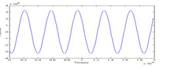
Direct digital synthesis (DDS) produces an analogue waveform, typically a sinusoidal wave, by generating a digital time-varying signal and then making a digital-to-analogue conversion. Since operations are predominantly digital inside a DDS system, it can offer fast switching between output frequencies, satisfactory frequency resolution, and operation over a wide range of frequencies. Several frequency generation possibilities are available to a designer, ranging from phase-locked-loop (PLL)-based very high-frequency synthesis techniques to dynamic digital-to-analogue converter (DAC) output programming to produce arbitrary waveforms at lower frequencies. But in both communications and industrial applications, the DDS approach is rapidly gaining acceptance for solving frequency (or waveform) generation requirements, since single-chip IC devices can produce programmable analogue output waveforms only and with high resolution and accuracy. In this FPGA project, we have implemented the high-precision Direct Digital Frequency Synthesizer (DDFS) used in digital up/down conversion, and the generation of periodic waveforms. For example, sine wave, cosine wave, square and sawtooth waves. The output is 16-bit signed data samples. This project is ideal for the quadrature signal generation, digital modulation/demodulation and software radio applications. Also, it can be used as oscillators and generation of complex quadrature signals.
Click here to download the FPGA source code

Figure 4: Sine Waveform
Optimizing Hashing Algorithms for Blockchain Systems
A cryptographic hash function is a hashing algorithm. It is a mathematical algorithm that maps arbitrary-size information to a fixed-size hash. In IT, cryptographic hash functions are used commonly. We may use them for digital signatures, authentication codes for messages (MACs) and other authentication types. We can also use them for indexing data in hash tables, for fingerprinting, identifying files, detecting duplicates or as checksums (we can perceive if a sent file didn’t suffer accidental or intentional data corruption). The algorithm for a hash function is designed to be a one-way function that cannot be reversed. Multiple hashing algorithms have, however, been corrupted in recent years. This FPGA project aims to provide the FPGA implementation of the hashing algorithms to generate the hashes for the Proof-of-Work (Pow). In this project, we have developed the Blockchain system to mine the 0xbitcoin. We have used the CVP 13 FPGA board and implement the Keccak-256 algorithm on it. We have achieved the 500 Giga hashes per second.
Click here to download the FPGA source code
Implementation of Radar Signal Processor on FPGA
High-performance digital electronic circuits for onboard processing of return signals in airborne precipitation – radar measurement devices in commercially available fields have been developed – programmable gate arrays (FPGAs). Previously, it was common practice to downlink the radar-return data to a post-processing ground station – an expensive practice that eliminates the near-real-time use of automated targeting data. In theory, a system of about 20 personal computer-type microprocessors could perform onboard processing; compared to such a system, the current FPGA-based processor is much smaller and consumes much less power. Alternatively, an application-specific integrated circuit (ASIC) may be used for onboard processing. However, compared to an ASIC implementation, the current FPGA implementation provides the advantages of (1) greater versatility for research applications such as the current one and (2) lower costs in the limited production volumes typical of research applications. Implementing the radar signal processing techniques on the FPGA is the significant domain. In this FPGA project, we have selected a few algorithms in the FPGA. Implement the Radar Equation along with the pulse compression algorithm, Implement Doppler shift to detect target velocity, and implement pulse-Doppler waveforms.
Implement a constant false alarm rate (CFAR) detection adaptive algorithm on FPGA used in radar systems to detect target signal against a background of noise, clutter and interference. Aim of this project to detect the target from a noisy condition.
Click here to download the FPGA source code
Fast Fourier Transform (FFT) on FPGA
The Fast Fourier Transform (FFT) is a fundamental building block used in DSP systems, with applications ranging from Digital MODEMs based on OFDM to algorithms for Ultrasound, RADAR and CT image reconstruction. Although its algorithm is straightforward to understand, for hardware engineers today, the implementation architectures and details’ variants are essential and are an enormous time sink. In this FPGA project, we have implemented the Fast Fourier Transform on the FPGA; we have used the butterfly technique to implement it on the FPGA. The FFT is used to perform the find the frequency component in a complex signals plan. It’s a 4096-point FFT. With device-level fixed point C-models, this FFT project core offers four different architectures and reduces the average implementation time from 3-6 months to the push of a button. It also gives users the opportunity to make complex trade-offs needed by both the DSP algorithm and hardware engineers for all the appropriate algorithms and implementation. The FFT project emphasizes increased dynamic range by growing the support for data and phase factor width up to 34 bits and supporting IEEE single accuracy floating-point data form. By using a higher precision fixed-point FFT internally to achieve comparable noise efficiency.
Click here to download the FPGA source code
Convert BCD to 7-Segment on FPGA
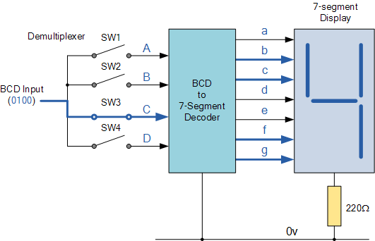
A Digital Decoder IC is a device that transforms one digital format into another, and the Binary Coded Decimal (BCD) to 7-Segment Display Decoder is one of the most widely used devices for doing this. 7-segment LED (Light Emitting Diode) or LCD (Liquid Crystal Display) style displays offer a very convenient way for numbers, letters or even alpha-numerical characters to display information or digital data. Usually, 7-segment displays consist of seven individual-coloured LEDs (called segments). The correct combination of LED segments needs to be illuminated on display to generate the necessary numbers or HEX characters from 0 to 9 and A to F, correspondingly, and BCD to 7-segment display decoders 74LS47 do just that. A Seven-Segment Display is an indicator widely used to show details to the consumer by FPGA designers. In VHDL code to convert from binary to compatible seven-segment display can be done quickly. Several applications may need one or more seven-segment displays to be used, i.e., counter, stopwatch, current measurement. In this cool FPGA project, we have BCD to 7-segment display decoder. The VHDL entity takes 4-bit BCD as an input and outputs the 7-bit decoded output for driving the display unit. A seven-segment display is being used to display decimal digits. They have LED elements which become active when the input is zero.
Click here to download the FPGA source code

Figure 5: BCD to Seven Segment Display
Digital Clock on FPGA
The digital clock’s primary purpose is to use the 7-segment panel on the Artix-7 FPGA Board to digitally display the time. By default, the digital clock shows the runtime and the time can be adjusted using the time set allocated to the onboard switch. The alarm role is also configured using the alarm set and the alarm on the kit’s switch. The developed digital clock is a format designed for 24 clocks. For the hardware implementation of the digital clock, this project uses FPGA. The clock starts as soon as the FPGA is turned on. The FPGA and onboard clock will produce the Timing signals. You can set the clock time and the alarm time using the dip switches on the board. Using digital operations: counting, comparing, increasing and decreasing, the suggested digital clock design is improved. Using the time set switch, the clock time can be set, and the alarm time can be set using the alarm set switch. If the clock is equal to the alarm time, the alarm will be on. By using the push buttons on the monitor, minutes and hours can be increased and decremented. In this FPGA project, we have implemented the Digital clock on FPGA. The module has one input “the source clock of the FPGA” and has 3 outputs (hour hand, minute hand, and second hand). We have displayed the output on the Seven Segment Display of the Artix-7 FPGA.
Click here to download the FPGA source code
JPEG Hardware Compressor on FPGA
Compression of image processing images can enhance the Device efficiency by minimizing cost and time to minimize without a significant reduction, image storage, and transmission of the picture’s quality. It is possible to describe a monochrome picture with each pixel over a matrix of picture elements (pixels), Described by the grayscale value of 8 bits. This depiction of Image data might require significant storage requirements. Compression of the image aims to decrease the size of the representation and, at the same time, to preserve much of the representation. It can be lossy or lossless compression. Compression with Lossy gives Compared to lossless, a higher reduction in data volume Compression; but just an approximation of the initial compression. It is possible to recreate the image. There are many norms for compression of images and Like Joint Photographic Experts Decompression (CODEC) Team, Format for Graphics Interchange (GIF), Portable Network Graphics (PNG), Picture Labeling Format of File (TIFF). The most commonly used JPEG compression. The type of lossy image compression used and based on the Discrete transform of cosine (DCT). Depending on the details found inside the image and the image, a compressed image in JPEG format may be approximately 10 percent of compression’s original size efficiency. The results in a reduction of 90 percent in the Bandwidth needed. This FPGA project includes a complete JPEG Hardware with 4:1:1 subsampling, able to compress at a rate of up to 42 images per second at the maximum resolution (256×256 @ 60 MHz). The FPGA input is RGB input (row-wise) and outputs to memory the compressed JPEG image.
Click here to download the FPGA source code
FM Receiver on FPGA
We built a simple FM receiver on the FPGA that demodulated the FM modulated frequency signal. We have used the dipole antenna to receive the FM signals then used the FM demodulator logic to demodulate the received signal. First, we used the ADC to convert the analogue FM signal to the digital and then process it digitally to remove the carrier waves to get an only pure sound wave from the broadcast station.
Click here to download the FPGA source code
Square Root on FPGA
In physics, the square root function sqrt(x) is an essential elementary function—Digital signal and image processing, ANN equations. The Field Programmable Gate Arrays (FPGAs) are currently being extended to solve the problem. Problems where the calculations of the function sqrt(x) are necessary. The FPGA manufacturers and third-party companies are proposing various IP cores of sqrt calculation (x). But these IP cores were developed decades ago and typically did not take the characteristics of the latest generations of FPGA into account. They do need upgrades, therefore. An enhanced feature algorithm to calculate sqrt (x) is suggested in this FPGA project, which fits the FPGA implementation I have written a code for finding the square root of a signed number on FPGA using VHDL as a programming interface. The code is based on “Non-Restoring Square Root algorithm”. The code takes one signed number, 32 bit in size and returns the square root, which is also of signed type with 16-bit size. The modified algorithm, CORDIC-like, for It is proposed to derive the square root equation. The algorithm is separated by the reduced sum of Steps proportional to the data given, and the outcome is Width of bits. In VHDL, the algorithm is defined and is Built to enforce the FPGA. This is the most Efficient at the floating-point throughout its implementation Module Square Root.
Click here to download the FPGA source code
Error Detection on FPGA
The detection of errors decides if the data obtained via a medium is Corrupted while transmitting. To achieve this, the transmitter uses a feature to measure and append the checksum value for the data Checksum for the original frame of data. To create a checksum for the received data frame, the receiver uses the same calculation technique and compares the received checksum to the transmitted checksum. If the two checksum values are identical, the data frame obtained is right, and there was no data corruption during transmission or storage. In this FPGA project, we have developed the CRC on FPGA to detect the error in the transmission message. The advantage of the CRC circuit generated is that the input is assumed to be serially fed into the circuit. Meaning, the input can be long and still the FPGA resource usage will remain the same.
Click here to download the FPGA source code
Ring Counter on FPGA
A ring counter is a kind of counter made up of flip-flops connected to a shift register, with the last flip-flop output fed to the first one’s input, forming a “circular” or “ring” structure. In hardware design (e.g., ASIC and FPGA design), ring counters are also used for constructing finite-state machines. A binary counter will require an adder circuit that is considerably more complicated than a ring counter and has a more significant propagation delay as the number of bits increases, whereas a ring counter’s propagation delay would be almost constant regardless of the code’s number of bits. In this FPGA project, a ring counter is implemented on the FPGA, consisting of a series of flip flops connected positively. The circuit is an especial type of shift register where the last flip-flop’s output is feedback to the first flip-flop input.
Click here to download the FPGA source code

Figure 6: Ring Oscillator on FPGA.
FPGA Implementation of AES-based Crypto Processor
Increased demand for data security is an undeniable fact. To achieve higher security, cryptographic algorithms play an essential role in protecting data from unapproved usage. In this FPGA project, we present a cryptoprocessor using Advanced Encryption Standard (AES). The AES is integrated with a 32-bit general-purpose 5- stage pipelined MIPS processor. The integrated AES module is a fully pipelined module which follows the inner round and outer round pipeline design. The results show that the presented pipeline version of the AES algorithm and the MIPS processor outperform traditional methods. At the operating frequency of 553 MHz, the proposed design can achieve the throughput of 58 Gbps, the latency of 240 ns, and the minimum power consumption of 76 MW.
Our design is implemented so that crypto instructions do not block the processor’s instruction fetch cycle even though the crypto co-processor is running simultaneously. By default, each instruction is fetched from the instruction memory unit and completed all its cycles on the MIPS processor if the instruction is designed for the processor. However, if the fetch instruction is not a MIPS instruction, it will be sent to the crypto co-processor in the next clock cycle after the decode stage. We incorporate crypto co-processors with MIPS and make this integration so that crypto co-processors run by the MIPS without disturbing pipeline stages. The main contributions of this project are as follows:
- The pipeline version of AES is implemented, obtaining high throughput, low latency, and low power consumption. • The integration of AES and MIPS is presented, which can run at different frequencies.
- The implemented AES acts as a cryptoprocessor controlled by MIPS instruction while it does not disturb the MIPS processor’s pipeline stages.
Click here to download the FPGA source code
SPI Slave Serial Interface Controller on FPGA
For synchronous serial communication between a host processor and its peripherals, the Serial Peripheral Interface (SPI) is mainly used. Due to its low pin count and full-duplex mode that can achieve data throughput in the tens of Mbps range, the SPI bus is often chosen. A 4-wire interface with two unidirectional data lines is used by the SPI bus to connect between the master and the slave. It supports one master on one bus with several slaves and allows the bit transferred to be versatile in the protocol. An SPI slave computer interface that provides full-duplex, synchronous, serial communication with the SPI master is implemented in this reference design. The SPI bus’s data size can be set to either 16 or 8 bits. All CPOL and CPHA- 00, 01, 10 and 11 are assisted by the SPI Slave Controller reference architecture. Three pins (clock, data in and data out) plus one pick for each slave unit are used in this design.
Instead of reading and writing to individual addresses, an SPI is a good option for communicating with low-speed computers that are accessed intermittently and transfer data streams. An SPI is an excellent option if we can take advantage of its full-duplex capability to send and receive data simultaneously. In VHDL, this design is implemented. The Lattice iCECube2TM Position and Route tool integrated with the Synplify Pro synthesis tool is used for the design execution. The architecture uses an ultra-low-density FPGA iCE40TM and can be targeted to other members of the iCE40 family.
Click here to download the FPGA source code
AXI4-Stream Protocol Interface on FPGA
Advanced eXtensible Interface 4 (AXI4) is a bus family established as part of the ARM Advanced Microcontroller Bus Architecture (AMBA) standard of the fourth generation. In 1996, AXI was first implemented in the third generation of AMBA, such as AXI3.
The AMBA specification specifies 3 AXI4 protocols:
AXI4: A data and address interface mapped to a high-performance memory. Capable of Burst access on devices mapped to memory.
AXI4-Lite: A subset of AXI that lacks the potential for the burst access. It has an implementation that is easier than the full AXI4 interface.
AXI4-Stream: A fast unidirectional master-to-slave data transfer protocol.
Xilinx Vivado helps with AXI4 interfaces to build a custom IP. You may connect these devices to the Zynq Processing System or other devices. The AXI4-Lite interface process will be protected by this paper, which is useful for implementing memory mapping registers. There are two global signals for any AXI component: the clock ACLK and an active-low asynchronous reset ARESETN. On the rising edge of the clock, all AXI4 signals are sampled, and all signal alterations must occur after the rising edge. For the transfer of address, data, and control information, all five transaction channels use the same VALID/READY handshake method. This two-way flow control mechanism means that both the master and the slave can control the rate at which the master and the slave move the data. The information source produces a VALID signal to indicate when the address, data or control information is available. The information destination produces the READY signal to indicate that it can accept the information. When all True and READY signals in a channel are asserted during a rising clock edge, the handshake completes.
