
The Ultimate Guide to FPGA Design Flow
17/02/2019, hardwarebee
This article describes the entire FPGA design flow along with the various steps required in designing an FPGA — from the very beginning to the stage where the design can be upload to the FPGA. But before that, let’s first introduce the FPGA technology very quickly.
A Field Programmable Gate Array, or FPGA, is a semiconductor device that comprises of logic blocks which are programmed to execute a specific set of functions. These programmable logic blocks are connected to each other with the help of an interconnect matrix. These interconnects are responsible for connecting the logic blocks and facilitating the flow of signals across the chip. This structure is arranged in the form of a two-dimensional array consisting of logic blocks, interconnects, and I/O blocks that connect it with the input and output signals. A logic block itself is composed of a look up table or LUT and a flip flop or FF and a multiplexer.
One of the major benefits of using FPGAs is that they are reprogrammable, meaning they can be modified to serve a function that is completely different from the one they were performing before every time the designer uploads a new code to the FPGA.
Find electronic design, board design and module design companies:
Find FPGA design companies:
Find embedded software companies:
FPGA Design Flow
The FPGA design flow comprises of several different steps or phases, including design entry, synthesis, implementation, and device programming. We will explore each of these phases in detail.
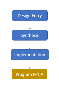
Design Entry
Design entry can be done using various techniques, such as schematics, through Hardware Description Language or HDL, or you may even combine the two and use a best of both worlds approach using tools that can convert HDL into schematics and vice versa depending on your FPGA design and preference. Generally, for a design that deals more with complex systems, it is better to opt for HDL, a quicker, language-based process that rids you of the need to design in lower level hardware, while schematics is a good choice for someone who wishes to design hardware because it gives more visibility to the entire system. You can also opt to go for a state-machines based approach, but it is largely limited and unused currently. It is suited for designers who view their design as a series of states.
There are benefits and downsides associated with each approach. While a schematic based technique is easier to read and comprehend, it tends to only work with relatively smaller projects. HDL based approaches, on the other hand, tend to be fast and easy to implement, and today is most popular design entry for FPGA designs.
Synthesis
After the design has been entered in the form of code, this phase is where it is translated into an actual circuit with elements such as gates, flip flops, and multipliers among others. Your input HDL is essentially converted into a netlist which lists the logic elements you will be needing for your project and the interconnects needed in the specific hierarchy.
The process begins with a syntax check once you feed in your HDL based design. It is then optimized by the reduction of logic, elimination of redundant logic, and the reduction of the size of the design while simultaneously making it faster to implement. The last step is to map out the technology by connecting the design to the logic, estimating the associated time, and churning out the design netlists which are subsequently saved.
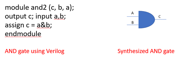
FPGA synthesis is performed by dedicated synthesis tools. Cadence, Synopsys and Mentor Graphics are EDA companies that develop, sell and market FPGA synthesis tools.
Implementation
This phase is where the layout of your design will be determined and consists of three steps: translate, map, and place & route. The tools used in this step are provided by the FPGA vendors because they know best how to translate a synthesized netlist into an FPGA.
The first step for the tools is to gather all the constraints that are set by the user together with the netlist files. These constraints can be regarding the assignment and position of the pins, the requirements regarding timing such as the maximum delay or the input period of the clock.
Then the tool maps out the implementation by comparing the resource requirement specified in the files to the resources actually available on the FPGA being used. The circuit is divided into the logic blocks or elements in the form of sub blocks. As a result, your entire design is placed in specific logic blocks and is ‘mapped out’ into the FPGA.
The next step is to connect and route all the signals accordance with the constraints set by the user between all the logic blocks and IO blocks.
Device Programming
The last step in the process is to finally load the mapped out and completely routed design into the FPGA. For that reason, you will need a to generate a BitSteam file.
FPGA Verification & Simulation
At the end of each step in the FPGA design flow, you have the opportunity to simulate and test you design. There are essentially 3 points allowed by the FPGA design flow: at design entry, post synthesis, or post implementation.
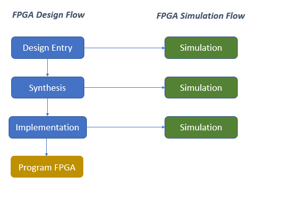
It is needless to mention that verifying that the implemented design performs the required funtionality an important part of the FPGA design flow.
Behavioral Simulation (At Design Entry)
Behavioral simulation, called also RTL simulation, is performed before synthesis. This fast simulation can be used to check the functionality of the design without constraints. Use this simulation frequently to test your code and find logic errors.
Functional Simulation (Post Synthesis)
The functionality the design can be verified using functional simulation after the synthesis process has completed. It is a netlist level simulation that ignore timing related issues.
Timing Simulation (At Implementation)
This simulation will give you the most accurate picture of your design behavior. It takes into account the target FPGA chip and all the logic blocks functionality, wiring, delays and much more. Timing simulation takes longer time and provides much more details than the previous simulation.
FPGA Design FAQ
Q: What is an FPGA?
A: FPGA stands for Field-Programmable Gate Array. It is a type of programmable hardware that can be configured to perform a variety of different functions.
Q: Why is FPGA design important?
A: FPGA design is important because it allows engineers and designers to create custom hardware solutions that can be easily changed or updated. This allows for greater flexibility in the design process and allows for rapid prototyping and iteration.
Q: What is the FPGA design flow?
A: The FPGA design flow is the process of designing and implementing an FPGA-based system. This typically involves creating a design in a hardware description language (HDL) such as VHDL or Verilog, synthesizing the design to generate a gate-level netlist, and then implementing the design on the FPGA using a place-and-route tool.
Q: What are the different steps in the FPGA design flow?
A: The steps in the FPGA design flow typically include design specification, design implementation, design verification, and design optimization.
Q: What tools are used in the FPGA design flow?
A: There are a number of tools used in the FPGA design flow, including hardware description languages (HDLs), synthesis tools, place-and-route tools, and simulation tools.
Q: How long does the FPGA design flow take?
A: The length of the FPGA design flow can vary depending on the complexity of the design and the resources available. Typically, it can take several weeks or months to complete the design flow for a complex FPGA-based system.
Further Reading: 10 Top Mistakes in FPGA Programming