10 Top Mistakes in FPGA Programming
14/07/2020, hardwarebee
This document provides a list of ten mistakes that are common in FPGA programming. We have collected 10 top mistakes FPGA design engineers typically make in their design and provides suggestions and alternatives which can be used as a solution for the same. This document assumes that the reader already has a base in RTL design and digital electronics. Let’s dig into 10 top mistakes to avoid in FPGA programming.
Having Asynchronous Logic
FPGA designs work well for synchronous systems, even though asynchronous logic is synthesizable, it can lead to timing violations in the design (metastability). Experience FPGA engineering tend to avoid having any asynchronous logic in their FPGA designs. A method to mitigate this problem is to synchronously latch all asynchronous logics in your design driving an LUT.
Asynchronous loops in your design can increase the power consumption of the FPGA which increases heat and could potentially lead to unnecessary thermal issues.
The following are cases where having an asynchronous logic is beneficial:
- In an AXI stream protocol, it is best to have “tready” as asynchronous, mitigating an asynchronous logic is possible here using a register slice but that increases the utilization for your entire design.
- DSP slice based calculations. Divisions, Multiplications using DSP slices can be done asynchronously with little to no effect on timing.
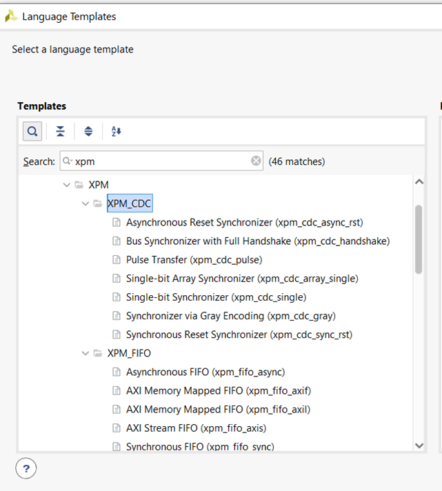
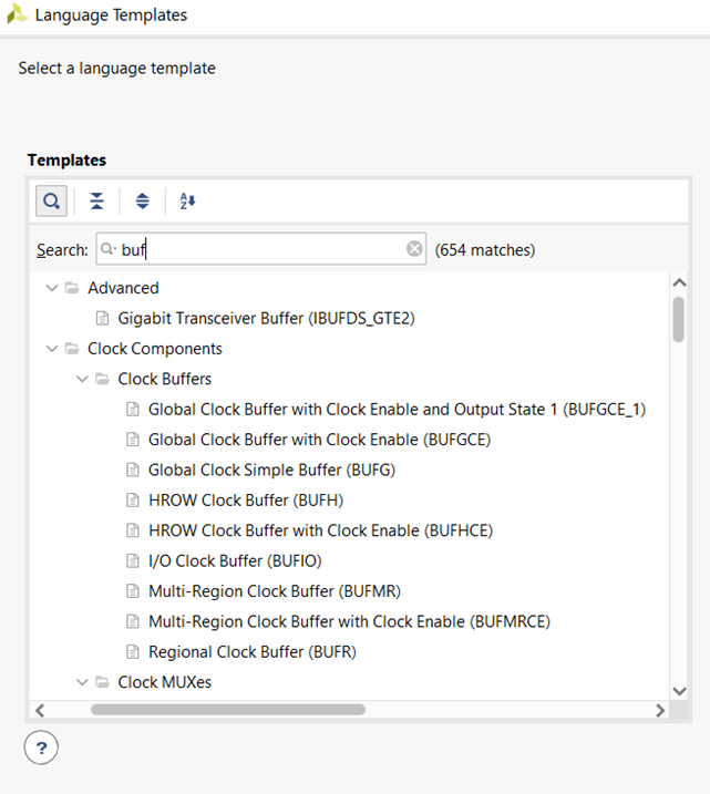
Not Using Primitives Provided on Device
This is a common beginner mistake in FPGA programming. Let’s take Xilinx devices for example, Xilinx provides primitives for clock buffers, CDC, DLL, clock dividers etc. making good use of the existing primitives in devices will lead to a more efficient design as well as drastically reduce the development time.
For example:
- Using xpm-cdc for a synchronizer will reduce the hassle of writing RTL for it as well as defining constraints for that signal.
- Using bufr for clock division will automatically place the generated clock on the clock tree, as well as infer the generated clock constraints.
Under-utilizing DSP Slices
In Xilinx FPGAs, DSP slices are capable of working as accumulators, adders, subtractors, dividers and multipliers. When needing these functionalities, it is better to use DSP slices rather than LUT’s/Fabric to perform this operation. This will reduce the time spent on design optimization as well as timing closure at the end of your design.
Some designs require very high clock frequencies for them to work, in such scenarios DSP slices can greatly reduce timing issues.
Checking for Inferred Latches in your Design
This is a case that can be explained well using an example. When writing a state machine, you are supposed to have 1 synchronous state and 2 asynchronous states. In the NEXT STATE LOGIC which is asynchronous, if you forget to account for all conditions, the tool will create an inferred latch, i.e. the next_state signal will be expected to be a generated clock in your design as it will be driving multiple LUT’s. Blindly ignoring such a scenario will cause the state machine to halt and not recover on board in the event of a glitch.
Not Running DRC Checks at Each Stage
DRC checks is a must and should be done after synthesis as well as implementation. Any critical warning in the DRC should be analyzed properly and should be accounted for in the design. Failure to do so can result in an unstable system that can fail at some point in time.
Not following Proper Naming and Coding Conventions
All RTL design engineers are expected to follow a standard naming convention for their designs such as.
- Adding i_ for all inputs
- Adding o_ for all outputs
- Adding s_ for all signals
- Adding c_ for all constants
- Adding g_ for all generic
- Clocks should be named as i_clk_<integer>m<decimal> : eg i_clk_122m88
- Resets should be named as i_rst_<polarity_<clock domain> : i_rst_n_122m88
Indentation guidelines such as 3 spaces for tabs are also expected.
All code should be properly documented, commented and tested (presynth as well as postsynth)
Unnecessary Usage if Reset Signal
In Xilinx devices driving all signals using a reset pin is not preferred as it drastically increases the fanout in the design. Instead it is preferable to use the gsr pin for all intermediate signals.
I.e : when declaring signals initialize it there itself to the reset value.
Refer to “https://www.xilinx.com/support/documentation/sw_manuals/xilinx2014_1/ug974-vivado-ultrascale-libraries.pdf” page 75
Calculation of Utilization
In FPGAs it is not recommended to completely utilize the all available resources. When starting the design, select a device that can hold your design with an additional 10% to 20% free space. This is done so that the router has leeway to clear up all the setup and hold time violations using its inbuilt logic.
Failure to do so will force you to work at a slower clock frequency to achieve timing closure on your design.
Using Block Designs for Large Designs
Block designs are a great way to interconnect RTL with ease, but for large projects a pure RTL project is more predictable and easier to debug. Block designs also have a lot of inherent bugs in Xilinx Vivado which will cause a lot of unnecessary warnings in your design.
Block design will also take a lot of time to open and top module will be cluttered.
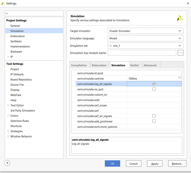
Not Checking Log all Signals Option in Simulation Settings
While simulating a design it is best to initially check the log all signal option in vivado. This will prevent you from having to rerun the entire simulation just so as to add an additional signal to the simulation waveform. This is applicable for all third party simulation softwares being used in conjunction with vivado.