SMPS Full Form
11/08/2022, hardwarebee
SMPS Full Form, sometimes referred to as Switching Mode Power Supply, is the full form of SMPS. A switching regulator is used by SMPS, an electronic power supply system, to efficiently transmit electrical power. In fact, SMPS full form is an electronic circuit that converts power which switches. These switches turn on and off at a high frequency, and storage components such as capacitors and inductors are used to supply the power. SMPS full form is a converter that converts AC/DC to DC. It can be said that the SMPS is an AC to DC converter, but a rectifier converts AC to DC, and a DC to DC is connected to the rectifier to complete the SMPS converter. In computers, often PSUs (power supply units) are utilized to adjust the voltage to the right range for the computer.
Apart from SMPS, there is another type of power supply, namely linear power supply (LPS), which is a non-switching technique by using linear regulators, and all transistors are working in their linear region. Some applications of this type of power supply are communications systems and low-noise amplifiers due to low output ripple, signal processing, and so forth. However, this power supply has some disadvantages, which lead us towards the SMPS. The main drawback is the efficiency of LPS which is in the range of 40 to 50 percent. The reason for low efficiency is that the transistor works like a variable resistor in LPS which dissipates the energy. Therefore, no resistor should be used in power supplies to enhance efficiency. Moreover, LPS is quite heavy due to big transformers and heat sinks which prevent them from being used in high-power applications. In LPS, the output voltage is always less than the input voltage and producing output voltage with reverse polarity is not possible. However, the SMPS efficiency is more than 85 percent which is much higher than the LPS efficiency because no resistor is available in the circuit, and only storage components (capacitors and inductors) and switches can be seen in the circuit, which reduces the dissipation considerably.
SMPS full form block diagram of and explanation
As mentioned, the first step in SMPS is the rectification of the source AC voltage together with an output capacitor to filter the rectifier output voltage. The next stage is the chopper which uses switches to create positive pulse voltages with a frequency of 20 to 100 kHz. The chopper is connected to a high-frequency transformer to step up or down the primary voltage. After changing the voltage level by the transformer, the secondary voltage is rectified using Schottky diodes. Then inductors and capacitors are employed to smooth the rectified voltage. In order to regulate the output voltage, a feedback circuit is used, and in the control circuit, the output voltage is compared with the reference voltage, which may have an isolation mechanism like optocouplers. The whole block diagram of the SMPS is shown in Figure 1.
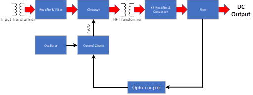
Figure 1: Block diagram of SMPS to convert AC input voltage to DC output voltage
Classification of SMPS Full Form
The SMPSs, which are DC/DC converters, can be classified as:
- Isolated SPMSs which use HF transformer
- Non-isolated SMPSs without any types of transformers
Examples of isolated SMPSs are flyback converters, push-pull converters, half and full bridge converters, and so on, which have HF transformers to control the output voltage. The transformers that are used in isolated SMPS are small and cost-effective as the transformer size and the operating frequency have an inverse relationship.
Buck converters, boost converters, buck-boost converters, cuk converters, charge pump converters, etc. are some examples of the non-isolated SMPSs which have inductors or capacitors as an energy storage device, and the output voltage is controlled by changing the duty cycle from 0 to 1 instead of HF transformer.
In this article, a charge pump converter (voltage doubler) as a non-isolated SMPS is discussed. For better understanding, principles are explained at first, and then the circuit is presented. Suppose there are a real voltage source and a load in the circuit, and the output voltage is higher than the input voltage. The aim is to increase the voltage using storage components and switches. To achieve this goal, two parallel capacitors can be used in the circuit, as shown in Figure 2.
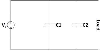
Figure 2: Parallel capacitors in the first stage
In this condition, when the capacitors are fully charged, the voltages of the capacitors would be equal to the source voltage. If the source is disconnected and the capacitors become in series using switches, the output voltage will be twofold, as shown in Figure 3.
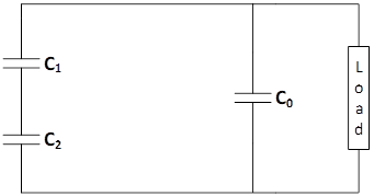
Figure 3: Series capacitors in the second stage without source
In fact, the output capacitor is charged and acts as a voltage source for the load. The real circuit for the charge pump converter is presented in Figure 4. As can be seen, there are four switches and three capacitors to increase the input voltage. The capacitors are mostly electrolytic ones, and the first capacitor is called Ci as it is connected to the input voltage. Two other capacitors are Cp and Co, which are called pump and output capacitors, respectively. The presented switches are turned on and off in a logical sequence to create the described conditions. When the input capacitor is charged, S1, and S2 are turned-on to create the parallel configuration between Ci and Cp. Once the pump capacitor is reached a certain value, the second sequence is started, and the mentioned switches are turned off while S1 and S4 turn on, connecting the Ci and Cp in series. For voltages lower than twice the input voltage, the second step can be started when the input capacitor is not fully charged. It is worth noting that the pump charge converter can produce output voltage with negative polarity by changing the configuration and switching logic.
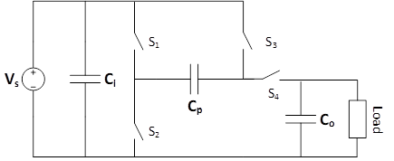
Figure 4: Charge pump circuit, including three capacitors and four switches
Advantages of SMPS
Some of the benefits of SMPS have been discussed in the previous section of this article, and in this section, more advantages are defined. The most important advantage of SMPS is efficiency which is more than 85 percent with smaller size with respect to the LPS. Since SMPS is compact, the costs of manufacturing are reduced. Moreover, no resistor is available in SPMS, which means that less heat will generate in SMPS. High power density and low weight are other advantages of switching power supply. It can be noted that the SMPS can produce output voltage higher than input voltage with various voltage steps, which increases the power supply flexibility, and it is less sensitive to variations of input voltage.
Disadvantages of SMPS
In SMPSs, the switching frequency is high, which increases the switching losses in different configurations. Moreover, radio frequency interference can occur in neighboring the circuit due to high-frequency operation. To solve this problem, both the input and output of the SMPS must have filters for controlling radio frequency noise. Another drawback of the SMPS is high ripple which can be 100 mV in some cases. Since the SMPS uses switches and a controlling system, the circuit is much more complex than the LPS, so expert design is required to overcome the possible issues, and the circuit is more expensive compared to the LPS. The switching system with high frequency can also produce harmonic distortion in the system, which is undesirable.
Applications of SMPS
A wide range of applications can be considered for SMPSs which are discussed in this section. One of the well-known applications of the SMPS is in the servers, computers, and power stations. They are also available in EVs or hybrid vehicles as battery chargers. Railway systems also have SMPS. Other applications are lighting and machine tool industries.
Example of a typical application
As mentioned, SMPS is used in many electronic devices. For example, keyboards, mouse, and other peripherals may be linked to a smartphone via USB. The USB port on the phone provides electricity to the auxiliary device. In this condition, a synchronous buck converter transmitting power both ways is used to regulate the power. When the phone is connected to a battery charger, the buck converter functions as a buck converter to charge the phone’s lithium battery. The buck converter operates reverse as a boost converter to produce 5V from the lithium battery when a peripheral is connected.


