What is FPGA?
08/07/2021, hardwarebee
What is FPGA?
FPGA stands for Field-Programmable Gate Array and can be defined as a hardware chip that is used to carry out logical operations. They are composed of an integrated network or sets of logic blocks placed across a chip; where the circuits are the programmable logic gates. FPGAs consist of individual configurable logic blocks, or CLBs, which are connected through programmable interconnects. As suggested by the name of the semiconductor technology, advantages of FPGA are known for their ability to be programmed when implemented in the field as opposed to other kinds of semiconductor chips (e.g ASICs) which are largely rigid in their design and execution.
FPGA Architecture
An FPGA is made up of an array of blocks called programmable logic blocks, these blocks are connected by configurable interconnect matrix. This means that both the logic behavior and internal routing can be programmed by the designer, giving the device its flexibility. The number of logic blocks is depending on the FPGA size (and price). The larger the FPGA the more logics blocks you could use. More logic blocks will allow you to use more “gates” and hence more functionality. The following diagrams show a general overview of FPGA architecture. Since the 1980’s and still today FPGAs are using the same architecture as shown below.
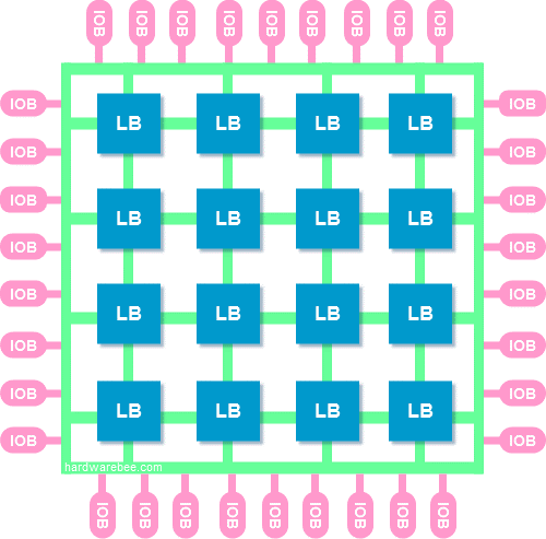
Figure 1: FPGA Architecture
The logic blocks and the interconnect structure are arranged in the form of a two-dimensional array and spread across the FPGA.
The following paragraphs describe the internal architecture of an FPGA:
Logic Blocks
Logic blocks are the fundamental elements in an FPGA that provide the logic function capabilities. An FPGA consists of many logic blocks that together can perform any possible logic implementation. A logic block is configurable and generally consists of a flip-flop along with a look-up-table and a muliplexer.
The following drawing shows a typical FPGA logic block architecture:
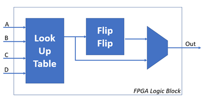
Figure 2: FPGA Logic Block Example
Input and Output Blocks
Input and output blocks are located next to every physical input or output pin. The IO blocks allow the user to select each pin functionality: whether it’s input, output or tri-state. And consist of some buffers and logic that are beneficial to have near the input or output pin. In some cases, the user can also control the signal slew rate to operate on fast or slow mode.
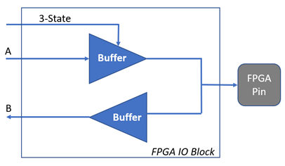
Figure 3: FPGA IOB Example
Using the internal routing, the signal is redirected in or from the IO block to the logic block.
Internal Routing
An FPGA chip’s internal routing is one of the most critical components of the device. It is the path that is used to connect all signals, as well as your clock to the different parts of your FPGA. The various logic blocks are connected to one another with the help of this internal routing which consists of channels comprising of interconnecting wires and electrically reconfigurable switches. These switches can be manipulated to connect and disconnect the various common logic blocks at different points and create a unique FPGA chip that is specific to your requirements.
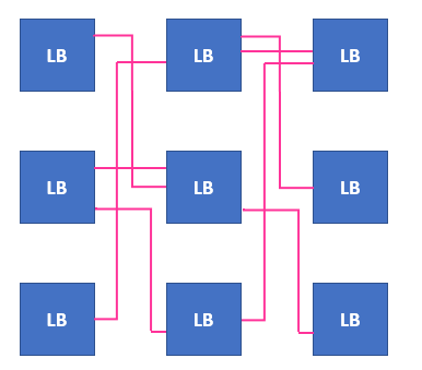
Figure 4: FPGA Interconnect Example
FPGA Design Language
When it comes to FPGA programming, one of the most important parts is the design language. This is the medium using which you will communicate with your technology and tell it what you want it to do. Using this language, you will basically be defining the operations of the hardware of that particular semiconductor chip and the device it powers. In the modern day, there are a huge number of computer design languages that can be used for this purpose.
Normally, you will use any hardware description language, or HDL, in the process of FPGA programming. You can use low level languages for circuits having relatively lower capacity. Higher end languages such as VHDL and Verilog which are used for higher complexity circuits and devices. Other factors that play a part in deciding which language to use include previous experience, personal preference and expertise, availability of models, synthesis capabilities, financial restraints, and hardware design.
Advantages of FPGA
An ASIC, or Application Specific Integrated Circuit for example, is designed to accomplish a particular task. As such, it will only perform that one function and cannot be modified to anything else, neither can it be erased and rewritten so as to reuse the chip. A new one must be created for a new purpose. An FPGA, on the other hand, can be reprogrammed and reused, and is much more flexible when it comes to customization and personalization, especially when deployed out in the field. This makes FPGA much more suitable and preferable over an ASIC in certain applications, which will be discussed ahead.
With the help of an FPGA , you can write a program which is loaded onto a silicon chip, and then execute the functions. If you want to optimize a chip, to fit a certain workload, then you can use an FPGA chip. Like mentioned before, FPGAs are field programmable and offer much more scalability and flexibility. They are able to keep up with modern requirements of high complexity and high performing devices. They also offer greater logic density, embedded processors, DSP blocks, and clocking among other prominent features.
FPGA are ideal for systems where consistent updates are a requirement. If a processor needs some changing, then FPGA chips can be used for making those changes if they are installed, eliminating the need to purchase new hardware. If FPGA chips are used in cars, then they can be updated with the help of these chips, even after they have been sold. These chips are also used frequently by enterprise businesses, because they can be reprogrammed using a data path that matches data analytics, image inference, and even compression.
The main purpose of an FPGA chip, at least originally, was for the prototyping of ASICs. The benefit of using an FPGA for this purpose is that it can be reprogrammed again and again, until a design is finalized and there are no bugs found in the design. Intel, a huge name in the IT industry, uses FPGAs to prototype new permanent chips so as to ensure their quality, function, and integrity.
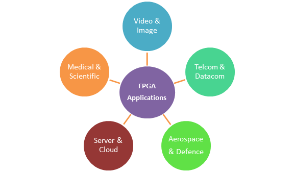
FPGA Applications
Since FPGAs work in a parallel fashion, they boast much higher speeds and thus can be used to solve complex computable problems, together with the re-programmability ability — this makes FPGAs both powerful and flexible machines. Some of the most common uses and applications for FPGAs today are:
- FPGA is being used frequently and extensively in communication systems to improve network capacity, coverage, as well quality of service while simultaneously reducing latency and delays, especially when it comes to the data manipulation. For example, in Server or cloud applications, companies are using FPGA extensively. Read here an article by Forbes about the usage of FPGA in datacenters.
Xilinx FPGAs are being offered by Amazon Web Services to accelerate compute intensive applications.
- The use of FPGA in automotive and vehicles allows application such as ADAR, LiDAR and autonomous driving. for a reduction in energy consumption, and improvement in efficiency, an increase in the power and communications systems, strengthened security systems, as well as a reduced overall cost. A very nice article by ElectronicDesign.com offer more details on how to integrate FPGA into the future car.
- In the business industry, the FPGA chips are opening up new doors for automation and secure technology which can help business owners and factory runners counter security threats and risks and enable the growth of automation in the workplace. Similar to the industrial hemisphere, FPGAs are also being used in the defense department for increased security, cyber or otherwise, as well as increased automation in vehicles and weapons.
- FPGAs are being used extensively over a wide range of other fields such as in medical equipment, computer hardware, and radio devices. They are also being implemented in the likes of bioinformatics, voice recognition technology, security and communications systems- wired or wireless, and in a number of scientific, medical, and consumer electronics.
- Since FPGAs have a large internal memory along with a great number of multipliers, they are being used as signal processing systems and digital signal processing applications. The logic blocks of FPGAs are being used for image and video processing.
- FPGAs are used for the purpose of hardware and algorithm acceleration as well as for accelerating artificial neural networks or machine learning applications as is being done Microsoft in their Project Catapult.
- These are ideal for use in low volume, vertical application productions as it may prove to be more affordable than an ASIC.
- The use of FPGAs is becoming increasingly more frequent as compared to microcontrollers for the Internet of Things as it allows fast processing of multiple aspects in a parallel and simultaneous fashion.
- They are ideal for use for high end control applications where an advanced degree of control is needed.
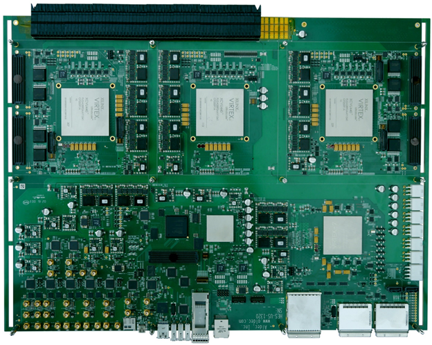
- ASIC emulation and verification can be done using FPGA (or several FPGAs connected on a single board). The FPGAs together can simulate and ASIC and allow engineers to perform testing and verification before they take the ASIC to production. The following image is showing a typical emulation board by Aldec.