
Xilinx vs. Intel High-End FPGA Series Comparison
28/05/2020, hardwarebee
This article provides a comprehensive comparison between the high-performance FPGA family of both Xilinx (AMD) vs. Intel (Altera) and will help you chose your next FPGA chip wisely.
The document is divided into the following subsections with numerous subsections which dive deeper into each topic:
- Feature comparison for high end Xilinx and Altera FPGA family
- Comparison of CLB and Clocking Structure
- Development tools overview
Feature Comparison of Xilinx vs Altera FPGAs
In this section we will be focusing on the most widely used high end FPGA from Xilinx (AMD) and Altera (Altera) which share the same category: ZCU11EG vs SX650.
- ZU11EG from Xilinx.
- Stratix 10 SX650 series from Altera (Intel).
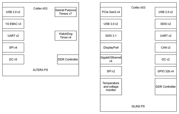
The PS section of both these FPGAs use the same 64 bit ARM A53 processor, with both devices boasting similar peripheral connections.
Even though similar Xilinx devices perform better than Intel devices in this group with a larger number of peripherals as well as better API support.
The most important feature comparison for PL would be look at the resources available on device. i.e LUT, RAM, MULTS, Clocking Structures.
Logic Elements available in both devices are :-
- Altera :- 612k LE + 207k ALM
- Xilinx :- 653k
Onboard RAM available in both devices are :-
- Altera :- 52Mb
- Xilinx :- 52.5Mb
A direct comparison is not possible for the multipliers available in both devices as the structure of multipliers are different for both architectures, but the comparable DSP slice numbers with Intel multipliers coupled with the floating point multiplication support on altera devices makes Altera the clear winner in multiplier capability.
As a personal opinion the choice of device should be based on your end product requirement, for 5G, RF or image processing based system it is better to use Altera chips which can make use of the large array of RF & 5G IP’s as well as the floating point arithmetic to make your life as a designer easy.
If the design is for video protocol implementation, fixed data manipulation I would prefer Xilinx devices with their advanced routing network which provides easy timing closure on your device and a better concept to market time.
Both vendors provide excellent support with a large community base to help you out regarding any problems you may face during the design.
CLB and Clocking structure
Xilinx CLB structure
The UltraScale architecture CLBs consist of the following elements
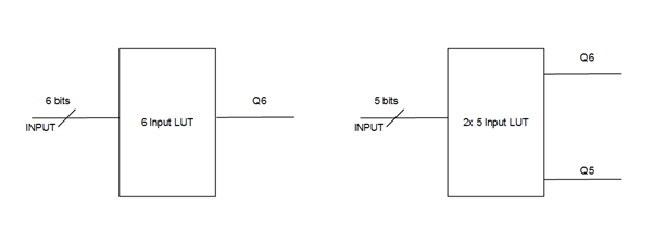
- Real 6-input look-up table (LUT) / Dual LUT5 (5-input LUT)
- Distributed memory and shift register logic (SRL)
- Dedicated high-speed carry logic for arithmetic functions
- Dedicated storage elements that can be configured as flip-flops(synchronous) or latches (synchronous/asynchronous) with flexible control signals.
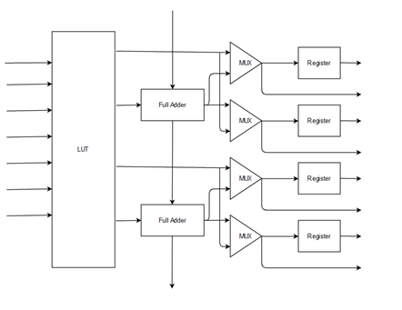
Arithmetic functions such as adders for upto 1024 bits can be performed in a single clock using the dedicated arithmetic routing.
LUT structure option is as shown below:
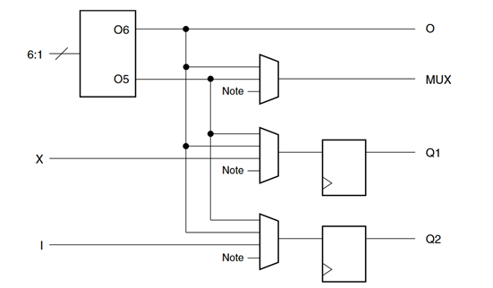
The entire structure of each CLB is depicted below:
Reference :- ug574-ultrascale-clb.pdf
Altera CLB Structure
The CLB / ALM structure in Altera’s devices are more complicated than what Xilinx devices have to offer. The high level ALM structure is represented below.
- Unlike Xilinx devices the Altera’s LUT is not capable of splitting itself to perform two separate architectures.
- The capability of the device to accommodate 8 bit LUT per ALM improves the routing time required for complex designs.
- Dedicated adders for arithmetic functions are identical with Xilinx providing a similar latency.
Xilinx Clocking structure
In Xilinx devices, the clock is managed using the Clock Management Tile which is placed in PHY next to each IO bank. This structure makes clock routing difficult across banks, SLR etc.
Each CMT contains 1 MMCM (capable of producing 4 phase synchronized clocks) and
2 PLL’s each capable of producing 2 phase synchronized generated clocks, thus each CMT can accept upto 3 external clock and generate upto 8 generated clocks.
The MMCM is the primary block for frequency synthesis for a wide range of frequencies, and serves as a jitter filter for either external or internal clocks
The PLL’s primary purpose is to provide clocking to the PHY I/Os, but can also be used for clocking other resources in the device in a limited fashion
Altera Clocking Structure
Clocking Altera devices makes use of programmable clock tree synthesis rather than the direct approach followed by XIlinx.
This technique uses dedicated clock tree routing and switching circuits.Clock tree synthesis minimizes clock tree insertion delay, reduces dynamic power dissipation in the clock.
This novel clocking structure enables Altera designs to be built faster than it’s Xilinx counterparts.
Development Tools
- The Xilinx IDE Vivado has slow compilation time whereas Quartus prime does not hog memory while providing faster synthesis and implementation results.
- For a concept to market model, Quartus will eliminate a lot of wasted time on simulation based validation
- Both development environment provides easy integration with version control systems
- Both IDE’s have inbuilt design helpers such as constrain editors for helping design engineers identify possible constraints for their design.
- Xilinx tools are much more heavily documented than Altera’s and thus the learning curve for using Vivado is much less than the learning curve for using Quartus.
Simulation Environment
Quartus prime uses the ModelSim while Vivado uses Isim as their default simulators.
Out of the both ModelSim fares a little better, but for industry grade projects most probably you will be using QuestaSim for all your simulation needs.
References
For further information regarding the devices please use the following links :
Altera:- https://www.intel.com/content/www/us/en/programmable/documentation/jzw1474049428757.html#joc1431448697339
Xilinx:- https://www.xilinx.com/support/documentation/user_guides/ug570-ultrascale-configuration.pdf