
Category Archives: FPGA Design
FPGA Engineering Services
23/03/2022, hardwarebee

FPGA engineering services are critical for the success of any complex FPGA project. This directory provides a comprehensive listing of companies offering FPGA engineering services.
When searching for FPGA engineering services, you should select a vendor that aligns with your organization’s technical and business requirements. Verify that the FPGA
FPGA Board Design
23/03/2022, hardwarebee
FPGA Board Design is a service provided by engineering companies to develop FPGA projects and designs.
An FPGA Board Design company will consists of a team of engineers who are educated and experienced in the field of FPGA engineering and have the necessary skills and knowledge required to ensure
FPGA Consulting
23/03/2022, hardwarebee
FPGA Consulting is a service provided by consulting companies to develop FPGA projects and designs.
An FPGA Consulting company will consists of a team of engineers who are educated and experienced in the field of FPGA engineering and have the necessary skills and knowledge required to ensure smooth development
CHIPS Alliance Forms F4PGA Workgroup to Accelerate Adoption of Open Source FPGA Tooling
21/02/2022, hardwarebee

SAN FRANCISCO, Feb. 18, 2022 – CHIPS Alliance, the leading consortium advancing common and open source hardware for interfaces, processors and systems, today established the FOSS Flow For FPGA (F4PGA) Workgroup to drive open source tooling, IP and research efforts for FPGAs.
FPGA vendors such as Xilinx (now part of
The Art of FPGA Debugging: How to Speed It up With Smart Design & Testing Tricks
04/11/2021, hardwarebee

Examples of FPGA projects based on Nvidia Jetson, Zynq UltraScale+, and Xilinx KRIA
Let’s try to optimize the most time-consuming stage of electronics design based on FPGA — we mean the FPGA firmware debugging. This article will talk about the 20/80 principle for the planning FPGA
FPGA Academy
31/08/2021, hardwarebee

Welcome to FPGA Academy
What is an FPGA?
FPGA Explained in Simple Words
FPGA Basics
FPGA Advantages and Common Applications
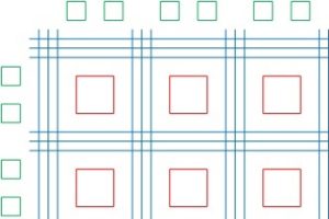
Introduction to CLB
The Ultimate Guide to FPGA
FPGA Architecture
FPGA Design Overview
FPGA Applications Overview
Getting Started with FPGA Programming
Overview of Look Up Tables in FPGA Design
How
What is FPGA?
08/07/2021, hardwarebee
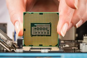
What is FPGA?
FPGA stands for Field-Programmable Gate Array and can be defined as a hardware chip that is used to carry out logical operations. They are composed of an integrated network or sets of logic blocks placed across a chip; where the circuits are the programmable logic
FPGA explained in simple words
07/07/2021, hardwarebee
Imagine a chip that can update its functionally unlimited times – exactly like an App on your phone. Welcome to the world of FPGA technology.
FPGA stands for Field-Programmable Gate Array, which is a chip that has programmable digital logic circuitry. The functionality of the digital logic circuitry is
FPGA Tutorial
26/06/2021, hardwarebee
Field Programmable Gate Arrays (FPGAs) are the the most efficient, cost-effective and reconfigurable solution for the hardware applications. It consists of re-programmable blocks which helps a user to reprogram for any given application.
The purpose of this tutorial is to focus on the FPGA design process and tools which
Intigia Joins HardwareBee Marketing Platform
23/06/2021, hardwarebee
HardwareBee, the leading marketplace for hardware service providers, announced today that Intigia, an engineering company specialized in dependable embedded systems: embedded software, hardware, and FPGA for safety critical applications, has joined HardwareBee to promote its engineering services. As part of the HardwareBee platform, Intigia will gain access to a full
Read More