
The Ultimate Guide to FPGA Architecture
01/03/2021, hardwarebee
This article provides a closer look into the history and the current FPGA architecture and it intended for electronics, FPGA and software engineers that would like to learn more about FPGA internals. The article discusses the traditional FPGA architecture and modern FPGA architecture. Also, it discusses the usage of internal logic functions e.g. Look-up-Table (LUTs) and internal routing element principals. At the end, the article addresses FPGA DSP blocks, FPGA timing, clocking architecture and modern high-performance FPGA architecture.
FPGA Architecture
FPGA stands for Field Programmable Gate Array, essentially it’s a piece of hardware that can be programmed as many times as the user wants and it can convert or implement any arbitrary equation into the form of the boolean equation, consequently, implement this as combinational and sequential logic. Simply put, an FPGA can be used to implement any logic function.
FPGA history commenced in 1980 when, Ross Freeman, created the first FPGA name XC2064, as shown in Figure 1, consist of an 8*8 grid of Configurable logic block (CLBs). From the original FPGA patent, one can see the basic structure of an FPGA. In this simplified FPGA, there are 64 CLBs. Each CLB has four inputs (A, B, C, D) and two outputs (X and Y). In between is combinatorial logic, which can be programmed to implement any desired logic function. The CLB also contains a flip flop, allowing the FPGA to implement sequential logic, i.e., counters, shift registers, state machines and other stateful circuits. There are multiplexers, which can be programmed to pass through any of their inputs to implement the combinational logic. The multiplexers allow the CLB to be configured for a particular task. Multiple CLBs can also be programmed to implement a single function. The intercommunication between CLBs can be done via interconnect architecture.
So, in short, each FPGA has the essential three fundamental elements that can be the core of modern-day FPGA architecture:
- Configurable Logic Block
- Interconnect Architecture
- Input/Output Blocks
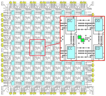
Figure 1: XC2064 First FPGA Architecture
Configurable Logic Block
The CLBs consist of three essential elements: LUTs, multiplexer, Flipflop. The LUT is the primary element that can implement the logical function, and a multiplexer is used to select the data output between combinational and sequential logic. Flip Flops is being used for sequential logic implementation, as shown in Figure 2.
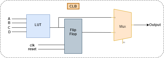
Figure 2: Configurable Logic Block Architecture
Look-up-Table
One of the most important element in an FPGA architecture is the LUT – it’s the core of the FPGA architecture. LUT is designed to implement any Boolean equation. Inside the LUT, there are multiplexers and the SRAM cells that contains the outputs based on the select lines. To implement a k-input LUT (k-LUT)—a LUT that can implement any function of k inputs—2k SRAM bits and a 2k :1 multiplexer is needed. Figure 3 shows a 3-LUT, which consists of 8 bits of SRAM and an 8:1 multiplexer implemented as a tree of 2:1 multiplexer. The 3-LUT can implement any function of 3 inputs (A, B, C) by setting the appropriate value in the LUT SRAM cells mask.
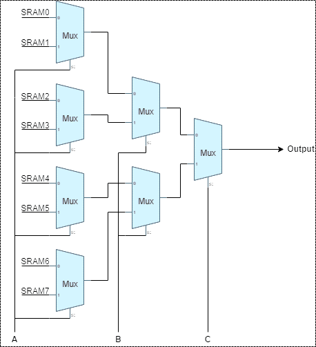
Figure 3: Look-up-Table Architecture
Interconnect Architecture
All the logic elements inside an FPGA are connected to an interconnect. The interconnect is a routing matrix comprises of programmable switches and wires. The routing elements provides a connection between Input/Output blocks, logic blocks, and between one CLB to another CLB. The programmable interconnect, as shown in Figure 4, consist of switches and wires for connection purposes.
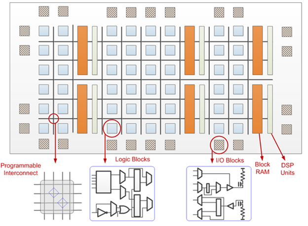
Figure 4: FPGA Architecture (courtesy Xilinx)
Input / Output Blocks
An I/O block is the input/output block that can be used for input and output both. The input and output paths contain edge-triggered D flip flops. The I/O blocks purpose is to provide the user interface from the outside world to the FPGA internal architecture. The I/O blocks comprise of the following items:
- Input from outside of FPGA to the FPGA pin.
- A delay element for the input, having an output for providing a delay to the input signal.
- A multiplexer is providing a delayed input signal.
- A register/latch is providing a register/latch output signal.
- A set/reset line for providing a set/reset signal
- A decoder for providing the set signal or the reset signal responsive to the set/reset signal.
- An amplifier has an output for providing an amplified signal to a related resource in the FPGA.
Modern FPGA Architecture
The modern-day FPGA architecture emphasizes the more and more LUTs in a smaller area with minimum power utilization, having more flexible on-chip memory. They are also focused on putting the adders/multipliers and DSP logic inside the CLB to reduce the latency, faster computation, reduced routing, and increased throughput. For many years 4-input LUT is the traditional LUT architecture design in practice. Xilinx has adopted a different approach to design a CLB that contains the two slices; each slice has four 6-input LUTs as shown in Figure 5 with two outputs and integrated with fast look-ahead carry logic and provide with better routing switches.
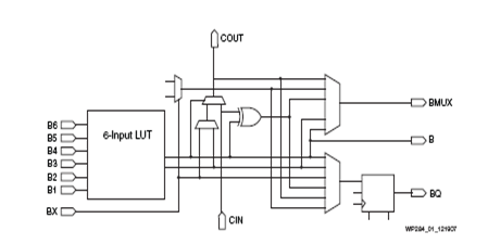
Figure 5: 6-Input LUT Architecture (courtesy Xilinx)
Clocking Architecture
As we have seen, to implement the logic on FPGA, we have two option either to implement the combinational logic and sequential logic. Sequential logic is essential, and the essential part of the design involves clock resources to be efficient, highly precise duty cycle, low power and jitter-free. Phase lock loop (PLL) and Delay lock loop (DLL) hardware has been incorporated with the FPGAs to generate the required frequency clock signals.
High-Speed Transceivers
To establish communication between the FPGA device and the external interfaces or devices, it is more convenient to use the high-speed differential connection instead of parallel to reduce the noise. Many standard protocols can be used for this purpose, like Ethernet, PCI Express.
FPGA DSP
The DSP48E2 was firstly introduced in Virtex–5 FPGA to make the multiplication and accumulation operation fast. This DSP tile’s generic feature includes a 27-bit pre-adder, 27 x 18 multiplier and a flexible 48-bit ALU that serves as a post-adder/subtracter, accumulator, or logic unit, as shown in Figure 6.
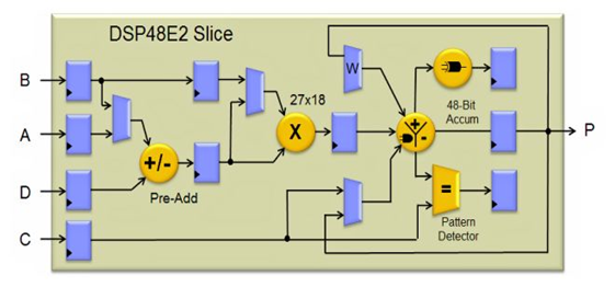
Figure 6: DSP48E2 Tile (courtesy Xilinx)
FPGA Timing
Timing is a term used in FPGA to refer to when it takes a signal to propagate from one flip-flop, through some combinational logic, to the next flip-flop. It is essential to understand that combinational logic is not instantaneous. It takes some time for the signal to propagate to the output. This is because digital circuits look like a bunch of RC circuits—Modern FPGAs based on CMOS technology, a type of transistor. The gate of a CMOS acts much like a capacitor and requires a small amount of time to charge and discharge the transistor. The more transistors you need to turn-on and turn-off, the longer it takes. Recall the metastability and debouncing theory; flip-flops require their inputs to be stable for a certain amount of time before and after the clock’s rising edge. These times are known as the setup and hold times, respectively. These constraints our circuit even more because we have to ensure that our combinational logic’s delay is short enough that the signal does not violate the setup and hold-time.
The modern FPGA not only contains the logic element but also equipped with memories, DSP blocks, clock architecture, transceiver to solve real-time problem in an efficient and timely manner.
Further reading:
A Quick Guide to FPGA architecture
FPGA Advantages and Most Common Applications Today
The Ultimate Guide to FPGA Clocks


