• Get Listed
    • Get a FREE Quote for your Next Project
HardwareBee
  • Find ASIC Vendors
  • Browse Design Services Directory
    • FPGA Design Services
    • Electronic Design Services
    • Embedded Software Companies
    • Add a Vendor
  • Get 3 Quotes From
    • FPGA Design Companies
    • FPGA IP Core Vendors
    • Electronic Design Companies
    • Embedded Software Companies
    • Design & Manufacturing Vendors
  • WikiBee
  • Resources
    • FPGA Academy
    • Embedded Academy
    • FPGA vs ASIC Calculator
  • Calculators
    • Watt to dBm Converter
    • dBm to Watt Converter
  • Emerging ICs
    • SPARK Microsystems – SR1000
    • Cologne Chip – GateMate
  • Pricing
    • Get Your Company Listed
    • Get Monthly Outbound Leads
    • Get Free Consulting
HardwareBee
  • Browse Design Services Directory
    • FPGA Design Services
    • Electronic Design Services
    • Embedded Software Companies
    • Add a Vendor
  • Get 3 Quotes From
    • FPGA Design Companies
    • FPGA IP Core Vendors
    • Electronic Design Companies
    • Embedded Software Companies
    • Design & Manufacturing Vendors
  • WikiBee
  • Resources
    • FPGA Academy
    • Embedded Academy
    • FPGA vs ASIC Calculator
  • Calculators
    • Watt to dBm Converter
    • dBm to Watt Converter
  • Emerging ICs
    • SPARK Microsystems – SR1000
    • Cologne Chip – GateMate
  • Pricing
    • Get Your Company Listed
    • Get Monthly Outbound Leads
    • Get Free Consulting
5022 Views

Quick Overview to FPGA Architecture

04/03/2019, hardwarebee

More and more companies are using FPGAs as a key component in their electronic product. If you are reading this article, you are probably interested in learning more about FPGA architecture.


So, let us dive into the very basics of FPGA architecture.


What is an FPGA?


An FPGA, or a Field Programmable Gate Array, is a programmable chip that can be reprogrammed in the field even after it has been programmed. It is a chip whose internal configuration is set by code that is determined by the FPGA designer. FPGAs provide an element of reusability as well as flexibility which is not the case with ASICs that are largely permanent chips that cannot be programmed once they have been produced.


An FPGA is like a white canvas, it can perform any digital function you can imagine, it offers versatility and flexibility that do not exist anywhere else.


On power up, the FPGA is loading its code from an external memory and then starts behaving based on the new functionality. An FPGA is SRAM-based; therefore, a code should be downloaded every time it’s powering up.


FPGA are used today in a wide range of applications. FPGAs can be found in following applications: Data Center, High Performance Computing, Industrial, Medical Products, Measurement Instruments, Video & Image Processing, Wired Communications, Wireless Communications, Aerospace and Defense, ASIC Prototyping, Automotive, and more. Let’s dive into the FPGA architecture and understand the internal elements that make FPGAs so special.


FPGA Architecture


An FPGA is made up of an array of blocks called programmable logic blocks, these blocks are connected by configurable interconnect matrix. This means that both the logic behavior and internal routing can be programmed by the designer, giving the device its flexibility. The number of logic blocks is depending on the FPGA size (and price). The larger the FPGA the more logics blocks you could use. More logic blocks will allow you to use more “gates” and hence more functionality. The following diagrams show a general overview of FPGA architecture. Since the 1980’s and still today FPGAs are using the same architecture as shown below.


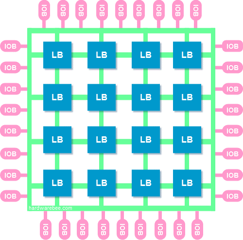
Figure 1: FPGA Architecture


The logic blocks and the interconnect structure are arranged in the form of a two-dimensional array and spread across the FPGA.


The following paragraphs describe the internal architecture of an FPGA:


Logic Blocks


Logic blocks are the fundamental elements in an FPGA that provide the logic function capabilities.  An FPGA consists of many logic blocks that together can perform any possible logic implementation. A logic block is configurable and generally consists of a flip-flop along with a look-up-table and a muliplexer.


The following drawing shows a typical FPGA logic block architecture:


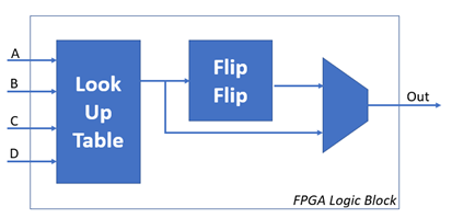
Figure 2: FPGA Logic Block Example


Input and Output Blocks


Input and output blocks are located next to every physical input or output pin. The IO blocks allow the user to select each pin functionality: whether it’s input, output or tri-state. And consist of some buffers and logic that are beneficial to have near the input or output pin. In some cases, the user can also control the signal slew rate to operate on fast or slow mode.


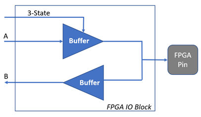
Figure 3: FPGA IOB Example


Using the internal routing, the signal is redirected in or from the IO block to the logic block.


Internal Routing


An FPGA chip’s internal routing is one of the most critical components of the device. It is the path that is used to connect all signals, as well as your clock to the different parts of your FPGA. The various logic blocks are connected to one another with the help of this internal routing which consists of channels comprising of interconnecting wires and electrically reconfigurable switches. These switches can be manipulated to connect and disconnect the various common logic blocks at different points and create a unique FPGA chip that is specific to your requirements.


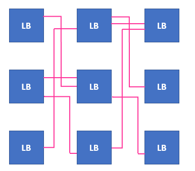
Figure 4: FPGA Interconnect Example


Further reading:


Top 10 FPGA Advantages

FPGA Advantages and Most Common Applications Today

FPGA vs CPLD

The Ultimate Guide to FPGA Clocks

FPGA History and Applications

Guide to FPGA Design Flow
FPGA Design Services Companies

linked in icon
Sign up for HardwareBee
* = required field

Recent Stories

5+ Best UWB Chipset Providers Compared
SPARK Microsystems Announces CDN$48 Million Financing Led by Idealist Capital
What is MicroLED? Overview, Benefits and Future
Auto processor market growing at 13% CAGR 22-28
The Ultimate Guide: Current Mirror
What is the Difference: GDDR5 VS. GDDR6
Watt to dBm (free) Converter
dBm to Watt (free) Converter
Get 3 Quotes from Electronic Design Companies
Get 3 Quotes from FPGA Design Companies
Get 3 Quotes from Embedded SW Services
Get 3 Quotes from EMS Companies

Find Design Services

Get Price Offers From
  • Electronic Design Services
  • FPGA Design Services
  • Embedded Software Companies
  • PCB Layout Services
  • Printed Circuit Board Manufacturers
  • Design & Manufacturing Services
Welcome New Vendors
  • Cologne Chip – GateMate
  • SPARK Microsystems – SR1000
  • TrigoPi
  • Fidus Systems
  • PCB Design
Answer a Question
  • Tips For Installing a PCB Prototype Board
  • Benefits of Working With a Reliable Flex Printed Circuit Board Manufacturer
  • FPGA company gross margin?
  • What is an FPGA used for?
  • When was FPGA invented
Recent WikiBee Items
  • Intel Quartus Prime
  • Static Timing Analysis (STA)
  • Look Up Table
  • Buck Boost Converter
  • Transimpedance Amplifier
Recent Posts
  • 5+ Best UWB Chipset Providers Compared
  • SPARK Microsystems Announces CDN$48 Million Financing Led by Idealist Capital
  • What is MicroLED? Overview, Benefits and Future
  • Auto processor market growing at 13% CAGR 22-28
  • The Ultimate Guide: Current Mirror
Most Popular Blog Posts
  • Promwad Accelerates Product Development with Vendor-Agnostic FPGA Design in Multiple Industries 
  • Understanding Knee Voltage
  • Understanding UPS Block Diagram
  • Understanding DV/DT in Electronics
  • Understanding Charge Pump

Never miss an update!

Follow us on LinkedIn

Do you need any price
information?

(Electronic design, FPGA design, Embedded SW services, PCB design, Turnkey)

Yes
No
HardwareBee

Copyright 2017-2023, HardwareBee. All rights reserved.

  • About Us
  • Contact
  • Subscribe
  • News
  • Get Free Support
  • Get listed
  • Send a wiki/article
  • Advertise

Follow Us

Be sure to follow our LinkedIn company page where we share our latest updates LinkedIn
Partner with us Partner with us

Design and Manufacturing Services

  • Engineering Design Services
  • Electronic Design and Manufacturing
  • Electronic Product Development
  • Electronic Product Design
  • Electronic Consulting Services
  • Electronic Engineering Companies
  • Electronic Engineering Services
  • Electronic Product Design and Development
  • Electronics Design Services
  • Electronics Design Company
  • Electronic Design Consultants
  • Electronic Design Company
  • FPGA Design Company
  • FPGA Consultant
  • FPGA Design Services UK
  • Electronics Manufacturing services
  • Electronics Manufacturing Companies
  • Electronic Contract Manufacturing Companies
  • Electronic Manufacturing Services Companies
  • EMS Companies Directory
  • Electronic Design Services
  • FPGA Design Services
  • Embedded Software Companies
  • PCB Layout Services
  • Printed Circuit Board Manufacturers
  • Design and Manufacturing Services