
The Ultimate Guide to FPGA
15/03/2021, hardwarebee
What is FPGA?
There are two general types of digital integrated circuits: ASIC and FPGA. ASIC (application specific integrated circuit) has a pre-defined one-specific hardware functionality which can’t be reprogrammed after manufacturing. FPGA (field programmable gate array) on the other hand can be programmed and reprogrammed after manufacturing.
FPGA is a type of integrated circuit that allows engineers to program customized digital logic, it’s a programmable chip that changes its hardware logic according the program. The main idea is to allow engineers to redesign and reconfigure their chips faster and cheaper and as often as they want to, however FPGA chips have limitations too — there is nothing ideal in the world!
FPGAs first appeared in 1980’s and their initial application was to allow the engineers to have general purpose programmable logic chip. This however required a lot of programming for being able to perform simple functions back then, so the engineers tried to avoid them as much as possible. But while in 1980’s FPGA was a simple interface device that was mostly targeted a glue logic which was hard to use for designing a complex system, it became a system-level integrated circuit with its own memory blocks, microprocessors and interfaces that allows designing serious systems.
Advantages of FPGA
FPGAs have several main advantages that make them unique:
- They enable engineers to build exactly the needed hardware, instead of having to use standard ICs or having to take the time, cost, and risk related to ASIC design.
- They allow doing operations in much faster, more energy efficient and more simple way compared to microprocessor or microcontroller.
- FPGA functionality can be updated like any other software code. Even if the hardware left the production site. This can help fixing bugs or adding new features.
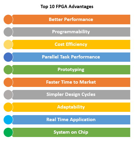
Figure 1: FPGA Advantages
Compared to microprocessors, FPGAs deal better with parallel tasks since microprocessors are sequential devices. However, microprocessors are more flexible when it comes to doing different tasks. FPGA does one specific task extremely good once configured while microprocessor does different things adequately.
Read more about FPGA advantages in this article.
CPLD vs FPGA
A complex programmable logic device (CPLD) is also a device that can be reprogrammed after being manufactured, it’s another type programmable device. In this sense they are similar to FPGA. However, there are significant differences as well. FPGA consists of many logic cells, while CPLDs are made of fewer logic cells. Due to their size, CPLDs are usually cheaper and faster. Nevertheless, CPLDs are very limited in their functions, they can’t be used for building complex systems, they are usually used in simple designs such as glue logic.
Read more about FPGA vs CPLD in this article.
Applications of FPGA
Applications for FPGA are many today. One of the examples is when we don’t know our requirements for sure during the manufacturing or they change with time. FPGA is one of the fastest and cheapest way of prototyping, but not limited to it. It is used for different purposes: from flexible design and machine-learning training to fast trading and crypto mining. Server application is one the latest application of FPGA devices.
However, they also have disadvantages such as:
- Hardware costs (but we believe this can change with time)
- Speed requirements (this will also improve as we go to deeper sub geometry technologies)
What to learn more about FPGA applications? Try this article.
Architecture and Building Blocks of FPGA
FPGA consists of building blocks that are like Lego pieces you can use to build your system. It has a basic logic building block called logic cells (CLB) shown below, but can also contain bigger other blocks like PLLs, interfaces, memories, etc. A single FPGA chip will have hundreds of thousands of logic cells (CLBs).
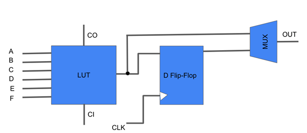
Figure 2: FPGA logic cell
We have a look up table (LUT) as a core of the FPGA logic block. LUT is a small memory that can implement any Boolean function by “remembering” it’s truth table. As you can see the output of the building block is multiplexed. One input of the multiplexor is a direct output from the LUT, which is used for pure combinational logic such as NAND, NOR, XOR or other logic gates. The other input of the multiplexer is the registered output of the LUT, after passing through D-type flip-flop and being stored synchronously with the clock.
One logic cell itself is a simple circuit that can’t do too much, but when there are many logic cells, we can implement any function we want. In order to do that the logic cell is being connected to an array of other logic cells. See the diagram below.
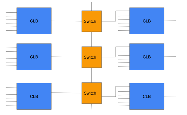
Figure 2: Conceptual simplified structure of an FPGA device
The orange rectangles between the CLB blocks in the middle of the diagram are the programmable switches that can route the output from a logic cell to anywhere. This is a very simplified diagram; in reality, there are many more wires and interconnects than shown here.
Pay attention to the carry in and carry out pins. Each adder is only one bit wide, while using the carry in/carry out pins it is possible to create large adders and counters very quickly and efficiently. Having fast, dedicated carry chains is one of the biggest advantages that FPGAs have over other programmable logic devices like CPLD for example.
In FPGA, a clock can reach all flip flops since digital design without clock is almost unimaginable. FPGAs have very advanced clock resources including a built-in configurable PLL (phase locked loop) and DLL (Delay Locked Loop). Since almost no modern digital design happens without multiple clocks with various frequencies and phase delays, clock management is very important.
FPGA also has input-output blocks for reading and outputting data. In addition to standard I/O blocks, most of the FPGAs have the following I/O features:
- Flip-flop output for synchronous I/O
- Differential signaling
- Double data rate (DDR)
- Serializers and deserializers (SERDES)
- Pull-up, pull-down, and tri-state I/O
- Adjustable slew rate, drive strength
FPGAs have built in memory like block RAM, distributed RAM (which can vary between 100Kb and 100Mb). The newest generation of FPGA devices also have DSP multiplier slices which are mostly used in DSP applications (digital signal processing). Some other built-in blocks that most of the FPGAs have are:
- ADC and DAC (Analog-to-Digital and Digital to analog converters)
- External memory controller such as DRAM, DDR, DDR2, etc.
- PCI Express controllers
- Ethernet MAC
- Dedicated FIFO
- High-speed transceivers
These blocks are designed on FPGA devices as “hard blocks” instead of being built by logic blocks and switches after the manufacturing process, because they are usually required by all complex systems. Since they exist in all the systems and are used very frequently, we want them to be there to save time (it does not make sense to design them from scratch using CLBs and switches all the time, instead we design them as a separate configurable block so that the designers can still change their parameters), but more importantly we want them to have very good characteristics, work very efferently and occupy less space. Moreover, some of these blocks have analog parts in them which require manual design and can’t be built only by digital cells.
Read more about FPGA architecture in this article.
How to Program and Configure an FPGA
Now let’s discuss the workflow of FPGA programming for building a system we want. In order to configure the FPGA, we need to program it. For programming FPGA hardware description languages such as Verilog, System Verilog and VHDL are used. These languages have some differences like Verilog data types being pre-defined while VHDL allowing a wide choice of data types (not necessarily pre-defined). Verilog is easier when it comes to syntax since it is similar to C language. All these hardware languages are equally effective for designing hardware devices. These languages are concurrent languages. This means that statements can be implemented in a parallel way similar to real life hardware. They are sequential languages too, since the statements are implemented one after another. They are also timing specific languages. While writing HDL code we should make sure that the code is synthesizable. Code’s syntax may be correct, but unlike software programming languages it also needs to be synthesizable. Verilog has different level of abstraction – from behavioral to register transfer and gate level. They describe circuits in a different level of abstraction. The workflow of defining hardware using FPGA is shown below:
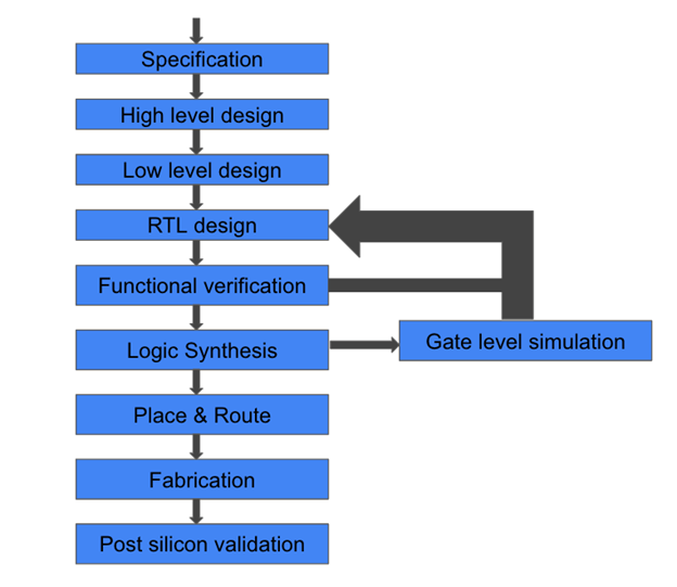
Figure 3: FPGA programming workflow using Verilog
Each one of the steps requires some toolset. Most of the FPGA manufacturers provide programming environment that has all tools needed. In order to start with FPGA programming, one should learn hardware design principles, description languages and tools used in the process. In the picture below, an FPGA design using Lattice’s Radiant software is shown:
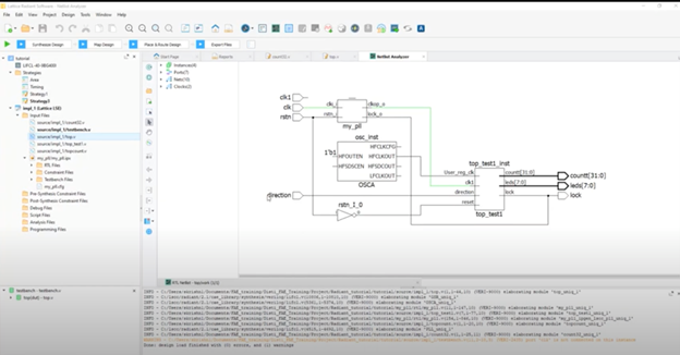
Figure 4: Lattice Radiant Software Tool Flow
More about FPGA programming in this article: How to start with FPGA Programming.
FPGA Manufacturers
FPGA is an industry worth billions of dollars. There are FPGA manufacturers that design and manufacture FPGAs. FPGAs differ from each other by technology (SRAM, Flash, Antifues), by configuration (Low-end, Mid-end, High-end), by node size (in nm), by vertical (based on their application industry) and so on. The biggest manufacturers are:
Each one of these manufacturers have their advantages and disadvantages depending on your application. In some complex applications a combination of FPGA from different manufacturers can be used as well. Get her a full list of FPGA companies.


