
Xilinx vs. Altera CPLD Comparison
08/04/2021, hardwarebee
This article discusses the difference between the Xilinx (AMD) vs Altera (Intel) CPLD architecture and their comparison. Also, this article discusses CLB architecture, clock generation, memory, and DSP operations of both Xilinx vs. Altera.
What is CPLD?
The design process to design complex system evolved drastically during the last 10 years. Usability of the programmable devices has increased tremendously. Electronic engineers starts implementing their logic circuits to on a simple Programmable Logic Array (PLA), Programmable Array Logic (PAL), then move to Simple Programmable Logic Array (SPLA) and then later move to Complex Programmable Logic Device (CPLD).
A CPLD chip includes several blocks of logic and wiring matrix to connect one block to another to facilitate the designer to implement a higher number of inputs and outputs required application onto the chip.
There are two major variants of the CPLD based on the manufacturer design strategy some fixed the AND array and left the OR gates programmable, and some with the contradictory approach with programmable AND gate and fixed OR gate. To implement the logic onto the CPLD, the designer must handy with the RTL languages, either Verilog or VHDL, and must have a toolchain provided by the vendor to apply the proper Placement and Routing strategy to have the final implementation of the design.
Applications of CPLD
The applications of CPLDs include the following:
- Complex programmable logic devices are ideal for high-performance applications and high latency require application where low latency is not required.
- CPLD can be used in digital designs to perform the functions of a boot loader.
- CPLD can also be used for loading the FPGA configuration data.
- Generally, these are used in small design applications like address encoding and decoding.
- CPLDs are frequently used in many applications, like in cost-effective applications.
- CPLD is beneficial to use small size and low power applications.
CPLD Selection Consideration
When considering a choice for the CPLD to use in design, some key criteria should be considered.
Programming technology
What kind of programmability that CPLD offers to you, either EPROM based? FLASH based or EEPROM based CPLD. SRAM, Antifuse technologies are also available for the CPLDs.
Function block capability
What are the functions block capability CPLD has and programmability?
I/O capability
The Input and Output capability, number of I/Os the CPLD can handle. The voltage level also involves in the selection criteria.
Density
You can find the size of CPLD required (logic density) for your design by submitting your design to the vendor software tool.
Performance
CPLDs come in a variety of speed grades so that you only pay for the performance you need. Use vendor CPLD software’s to determine the speed grade you need to meet your system timing requirements.
Voltage and Power
Different CPLD families have different voltage (supply and I/O) and power (standby and dynamic) offering.
Packaging
CPLDs come in a range of package types, from inexpensive QFP packages to ultra-small chip-scale pages, to high-I/O-count BGA packages
Based on the mentioned above parameters, an FPGA designer can choose to go with CPLD that suits best to the project requirements. Next, in this article, we will debate the Xilinx vs Altera CPLD architecture and their benefits.
Altera’s CPLD
The first-ever CPLDs was manufactured by Altera. First in their family of chips called Classic EPLDs, and then in three different series, named MAX 5000, MAX 7000 and MAX 9000. Because of a rapidly growing market for programmable devices, other developers developed devices in the CPLD category, and there are now many choices available, e.g., Microsemi, Xilinx. Here, the discussion will focus on the MAX 9000 series for Altera because it is commonly used and propositions state-of-the-art logic capacity and speed performance. The MAX 9000 represents an older technology that offers a cost-effective solution.
The generic architecture of the Altera MAX 7000 series is shown in Figure 1. It contains an array of blocks called Logic Array Blocks (LABs) terminology used by the Altera and interconnect wires called a Program Interconnect Array (PIA). The PIA can connect any LAB input or output to any other LAB to implement the complex functions. This is how the routing works between different logic blocks. The IOs of the chip connect directly to the PIA and LABs. The LAB can be thought of as a complex CPLD-like structure, and so the entire chip can be considered an array of CPLDs. The MAX 7000 devices are available both based on EPROM and EEPROM technology.
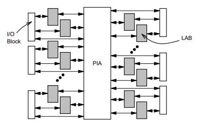
Figure 1: Altera Max 7000 Series
Xilinx’s CPLD
Xilinx is mostly an FPGA manufacturer; but they also offer a selection of CPLDs. Their most famous CPLD is called XC9500. Each XC9500 device consists of multiple Function Blocks (FBs) and I/O Blocks (IOBs) fully interconnected by the Fast CONNECT switch matrix. The IOB provides buffering for device inputs and outputs. Each FB provides programmable logic capability with 36 inputs and 18 outputs. The Fast CONNECT switch matrix connects all FB outputs and input signals to the FB inputs. For each FB, 12 to 18 outputs (depending on package pin count) and associated output enable signals to drive directly to the IOBs. Figure 2 shows the XC9500 Xilinx CPLD architecture.
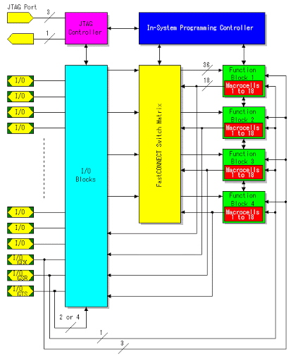
Figure 2: Xilinx XC9500 CPLD Architecture (courtesy Xilinx)
Altera vs Xilinx CPLDs
In this section, a comparison between Altera vs Xilinx CPLD is provided. For the comparison, A device from XC9500 family is chosen (XC95288) and a device from the Altera MAX7000 series was chosen (EPM7256E). Both devices have great potential and features to overcome one another. For example, the Altera CPLD have fewer resources but can run at a higher frequency. The Xilinx devices run at lower frequency but provide a lower output and pin to pin delay. In the case of resources, Xilinx has a better depth compared to Altera and can handle more complex operation. It depends on the designer, and the application requirements to choose which one to use, depends on either higher resources are the constraint or higher speed.
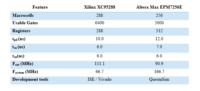
Table 1: Comparison between Xilinx XC95288 vs Altera EPM7256E


