
Ultimate Guide: FPGA Programming
27/04/2021, hardwarebee
In this paper, we covered all topics related to FPGA programming. The paper starts with an introduction to FPGA and its programming languages. And thereafter, takes the reader into the process of FPGA programming with a very basic HDL code that is used to demonstrate how an FPGA is programmed.
Normally digital design circuits are based on building blocks called logic gates. The logic gates are defined as physical devices that implement a Boolean function such as AND, NOT, XOR, NAND etc. When these Boolean functions are arranged in a certain way, a required function is achieved and resulting digital HW is then used throughout its life with that function. These hardware devices are called ASICs (Application Specific Integrated Circuit). They are called ASICs because they are specific to a certain function and cannot be changed later to implement a different function using same logic gates. However, an FPGA is a device that allows these logic gates to be arranged and rearranged several times, thus they can implement different functions throughout their life. And thus, their name includes Programmable Gate Arrays i.e. arrays of programmable gates. The word Field comes from the fact, that they can be reprogrammed even when they are out in field i.e. installed at some customer site. This gives an added benefit that HW updates can be viewed as SW updates and customers do not have to change their HW with any new update/features required.
The building blocks of any FPGA are logic gates (to implement the required functions/sub-functions), wires (to connect different logic gates), registers (to allow HW work at higher clock speeds) and memories (to store/retrieve the data). These elements within the FPGA are collectively called core or fabric of the FPGA (green and blue in the figure below). Depending on the family and vendor of the FPGA, the core/fabric can be arranged in different way to allow designers to implement the required function/system.
In addition to core, modern FPGAs are also equipped with hard IPs (shown in Grey boxes in figure below). The hard IPs are components/HW blocks that are there to perform dedicated function for example, a DDR controller to allow writing/reading the external DDR memory and transferring the data to the core of the FPGA. Some example of the hard IPs are processors, ADCs, DACs, DSP blocks.
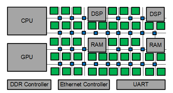
Figure 1: Modern FPGA architecture
FPGA Programming Languages
So now we know that FPGAs are different logic gates/elements connected together which can be configured as per requirements to create a HW to perform special function, but how we can configure those blocks/elements in a specific way. The specific language to implement those functions can be either Verilog, System Verilog or VHDL. All these languages are Hardware Descriptive Languages (HDLs) since they are used to describe how the digital HW should look like. All these languages can model the digital HW in 3 different abstraction levels.
- Behavioral Model
- Register Transfer Level
- Gate Level
Verilog is very close to C language in terms of syntax and operators etc. The first IEEE standard for Verilog was put out in 1995 (IEEE Standard 1364). System Verilog is the derivative of Verilog which gives much more flexibility and extension/features than Verilog and is used quite extensively for verification in industry. VHDL is quite different than Verilog/System Verilog in syntax but share quite many features in terms of functionality.
HDL vs Software Languages
All these Hardware Descriptive Languages are quite different to SW programming languages in terms of their execution. In contrast to SW languages, where the execution of a defined program is run sequentially (one statement executed by another), the HDL language defined programs execution is mostly in parallel. This parallel execution makes quite easy to model digital HW in these languages since in HW most of the things are running in parallel. To work/design HW using these languages, one must have a very good understanding of the logic design since in these HDLs, one is actually modelling the actual HW he/she intends to build. In FPGA programming the designer is programming a digital circuit.
FPGA Design Flow
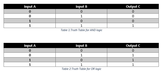
In digital logic design a signal can have only two values, Boolean 0 and Boolean 1. One should have a good knowledge of Boolean algebra to understand digital design. For example, Boolean AND and Boolean OR operations take in two values and provides one output value with truth tables as given below.
One of the most important concepts in digital logic is difference between combinational and sequential logics. Combinational circuits are the ones where output of the design is purely dependent on current values of the inputs. Sequential circuits are the ones, where the output logic is dependent on some feedback path (previous values) as well. A simple adder where HW calculates the sum of two inputs is an example of a combinational value. Since you only need to know the inputs to calculate the output. However, a counter which counts up (or down) needs to know the previous output to increase (or decrease) the value. In sequential circuits, one must use a Flip Flop to store the value of output temporarily to be used as input next time.
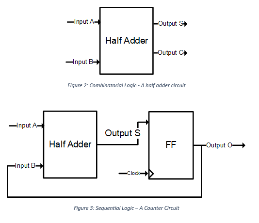
Once you know the type of circuit you want to create, we can try to describe it using any HDL. Here we can try an example in VHDL. We can take an example of Half Adder. The first thing is to create an entity in VHDL describing the module/circuit you want to create.
entity half_adder is
port (
A : in std_logic;
B : in std_logic;
—
S : out std_logic;
C : out std_logic
);
end half_adder;
Now to define the internal of the module, we need to know the truth table of half adder which can be found below.
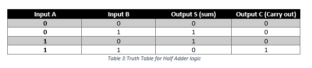
Now if we try to write output S and C in Boolean equations:
S = A´.B + A.B’
C = A.B
Where A’ represents a negated value of A, B’ represents the negated value of B, + represents the OR gate and . represents the AND gate. The equation for S can also be viewed as an XOR function between A and B.
Now we know the detailed HW structure, we can define the architecture (internals) of the already defined entity.
architecture rtl of half_adder is
begin
S <= A xor B;
C <= A and B;
end rtl;
The next step in this FPGA design flow is to verify that the design works according to specifications. One can create a testbench and provides different inputs to observe expected outputs. This is normally done by running the simulations of the HDL module in a simulator. There are several simulators used in industry provided by different vendors such as Mentor Graphics and Cadence.
Once the design is verified, the next step in the flow is to synthesize the design for target FPGA technology. Different FPGA vendors provide their own tools. Two of the biggest vendors for the FPGAs, Xilinx and Intel provide VIVADO and QUARTUSII respectively. These tools take the modules defined via HDL (Verilog/SV/VHDL) and synthesize/map them to the target FPGA. During the synthesis phase, the tool figures out all the logic elements required and all the connections between those logic elements. During the mapping phase, the tool maps those logic elements to actual configurable blocks within the FPGA along with configurable routing blocks to connect the design. In addition to the HDL defined modules, we should also provide timing constraints (if any) as well as pin locations for the inputs and outputs defined for the top module. Once the complete process is done, the tool creates a bit stream which can be downloaded in the FPGA (usually via USB). This bit file is complete configuration file for all the configurable logic elements within the FPGA.
FPGA Development Boards
Anyone willing to start/understand FPGA designs there are many FPGA development boards available in the market (such as Basys3 or Artix-7) . These FPGA development board normally comes with an FPGA, some LEDs (for visual outputs), DIP switches (for control inputs), USB, ethernet ports along with all the circuitry necessary to power up and run electronics. They also come with a lot of documentation to help and guide how to use and control FPGAs.
Tips and Tricks
- Start with something very simple in learning FPGAs like “Hello world” program in C
- If you are working with sequential circuits, one should be aware of how clocking should work in FPGAs. Clocks have special nets in FPGAs (not using normal routing configurable blocks).
- Familiarize yourself with the target FPGA technology to understand how configurable blocks look like and how they will be mapped into the design.
- Working with FPGA development board can be quite challenging in start but normally they come with tutorials which can be followed quite easily to get started.
- Always verify your design in simulations before running it on FPGAs as it will take long debugging sessions just to understand the issue within FPGA.


