


This website uses cookies so that we can provide you with the best user experience possible. Cookie information is stored in your browser and performs functions such as recognising you when you return to our website and helping our team to understand which sections of the website you find most interesting and useful.

FPGA Basics
07/05/2020, hardwarebee
This document introduces the reader to one of the articles we have created to help with FPGA Basics. This article will enables FPGA designers to get through the first basics steps of FPGA programming.
FPGA Basics
As FPGA designs get more and more complex, therefore it is very important for FPGA design engineers to follow a common set of rules and guidelines which make both design and debugging easier and generate bug free designs.
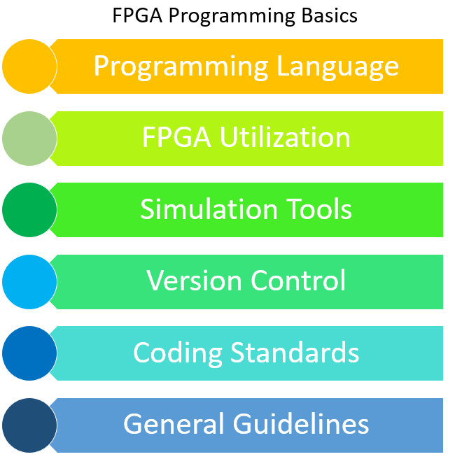
The first things to consider before starting an FPGA design are:
- FPGA programming language selection
- Estimate the FPGA resource utilization
- Simulation tools to be used
- Version control tool to be used
- Using globally acceptable coding standards
- Miscellaneous FPGA Programming Guidelines
1. FPGA Programming Language
For FPGA designs, nowadays one can use the following programming languages:
- VHDL
- Verilog
- High level languages (system C, Python, C++ etc)
- Generate RTL from tools such as MATLAB.
The Choice between RTL languages such a VHDL, Verilog and the rest is based on how much control you want over a design. If design optimizations are not of concern then high level languages provide the fastest ”Design to Market” time. This document will not be focusing on these methodologies. Between VHDL and Verilog the following should be taken into consideration before finalizing a language.
VHDL
- Strict language, hence very low chance of design functioning in any unintended ways.
- Timing simulation is not possible, hence timing should be taken care of using STA.
Verilog
- There is a chance of design failing post-synthesis functional simulation because of the flexibility of the language.
- Timing simulation as well as functional simulation is possible.
2. Estimate FPGA Utilization
Once an overall block diagram of your design is ready, you can have an estimate of the resource utilization. Always plan in such a way that the design never crosses 80 percent total resource consumption for your selected FPGA. This will drastically decrease the time required for timing closure for your design.
Following are the thumb rules for resource estimation:
- Understand the architecture of the FPGA platform being used correctly.
- Draw a block diagram for each module of your design and estimate the LUT,FF,DSP Slice and BRAM/URAM required for that RTL module for the architecture you have chosen.
- For IP’s being used in your design, Refer to the data-sheet for the resource consumption or you can perform an OOC build to get the utilization.
- Estimate the resources for synchronizers being used in your design.
- Lay a 10 percent leeway to the 80 percent utilization mark.
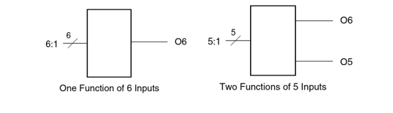
Note: LUT example based on Xilinx Ultrascale Architecture
The UltraScale architecture LUTs can be configured as shown below
- One 6-input LUT with one output.
- Two 5-input LUTs with separate outputs but common addresses or logic inputs.
3. FPGA Simulation Selection
We will be discussing on two tools in this document:
- Vivado Isim
- Questa Sim
Vivado Isim
This is a free simulator integrated with vivado. It is not the not robust simulator available. The ISIM is slower compared to Questa and is not suitable for long run simulations.
Questa Sim
If you or your organization have the funds to purchase a simulator, then I will recommend Questa just because of the sheer amount of time you can save in simulations.
4. Version Control Tool Selection
I understand that version control is not properly evolved for FPGA based designs, but it is imperative that you stick with a good VC such as GIT from the beginning of your project.
For Xilinx Vivado based designs, Xilinx provides very good documentation regarding integrating vivado designs with version control systems.
Correct understanding of ”UG1198-vivado-revision control- tutorial” will be a very good starting point for version control with xilinx designs
The below image represents a good folder structure for version control.
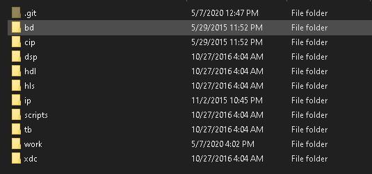
Where:
— bd : To store Block Design (.bd) files
— scripts : To store vivado run scripts and Makefiles
— hdl : To store VHDL/Verilog HDL including the top-level design
— ip : To store all XCI and XCIX files
— tb : To Store all testbench files .sv files should be wrapped in verilog files
— xdc : To store Xilinx Design Constraints (.xdc) for the top-level design
— hls : To sore all files related to C++ designs
— dsp : To store all Matlab SysGen design files
— work : Working directory for latest project to be committed to git
5. Using Globally Acceptable FPGA Coding Standards
Coding standards are very important as they make your code clear and professional.
Before we get into coding standards, let us finalize on a text editor and documentation strategy for your design.
I personally recommend using EMACS as your default text editor for any and all design purposes. The next best option will be VIM.
These editors let you stick with the logic only while they have commands for all repetitive constructs in your code and believe me, your choice of text editor for your
design will determine the amount of effort you put into writing your code.
Documentation is left out by many engineers to be done at the end of your design.
It is a much easier method to use a system like doxygen to prepare your documentation. It will reduce a lot of hassle and along the way make your design a lot more professional.
Following are a couple of good coding standards to be used in a design:
- Clocks should be named as (clk_<FREQ>). Eg clk_122m88
- Signal should start with ”s”
- Inputs should start with ”i”
- Resets should indicate clock domain and polarity. Eg rst_n_122m88
- Outputs should start with ”o”
- AXI naming conventions should be followed.
- One VHDL file should contain only one Entity and one Architecture
- Make sure each RTL file is synthesized independently and a post synthesis functional/timing simulation is performed.
6. Miscellaneous FPGA Programming Guidelines
Following are some points to keep in mind before starting your design:
- You should have a clear outline of clock domains as well as CDC techniques to be used for the design.
- In vivado use clock network analyzer to find possible CDC issues
- SSO Analysis is always performed.
- DataFlow analysis should be done prior to finalizing design so as to prevent any bottlenecks.
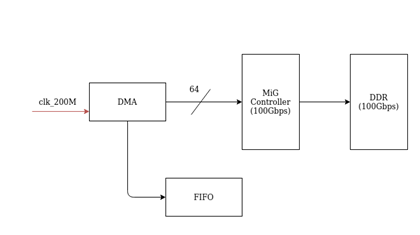
In the scenario shown below:
I . DDR and MiG has a throughput capability of 100Gbps
II . DMA clocked at 200 Mhz with 64 bit bus can support only 200*64 Mbps => 12.5 Gbps which is a bottleneck in the design.
III. To circumvent this bottleneck increase the width of DMA to 512.
- Define the clocking and reset strategy early in the design.
- Make use of primitives whenever possible.
- Use safe state machines.
- Handling of all FPGA Mode/Control pins (e.g. pullup/pull-downs) should be reviewed
- Minimize the use of asynchronous logic in your design
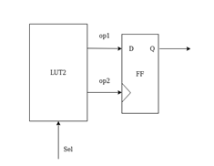
- Make sure that LUT’s are not driving clock pins unnecessarily.
For example a scenario as shown should be avoided whenever possible:
- If timing is not met at the end of the design try changing the implementation strategy to ”Performance-Retiming” in Xilinx devices.
- Validate each RTL using TB and store the simulation reports for each RTL. This should always be included in your documentation.
Sign up for HardwareBee