The Ultimate Guide to: Schematic Diagrams
20/05/2021, hardwarebee
One of the most fundamental aspects of electronic engineering, since its early days, is the schematic diagrams. Schematic diagrams is the most efficient way to represent a project on paper, and it can be used to perform circuit analysis, to supply information to simulators and layout editors, and for documentation purposes. Therefore, creating electrical schematic diagrams and reading schematics are fundamental skills for any electronic engineer, technician, and hobbyist. Here in this article, you are going to learn how to draw and read electronic schematic diagrams, free and commercial schematic tools, and good practices to improve the readability of your projects and optimize your design flow.
Schematic Diagrams Overview
Schematic diagrams are functional representations of electric circuits. Electric circuits, especially for electronics, are composed of many components, with different sizes, structures, colors, and packages. Besides that, the distribution of components and connections are dependent on the layout design, which varies greatly from project to project. Therefore, it is very difficult and often impossible to conceptualize and understand the functionality of a circuit without drawing schematics.
Electrical schematic diagrams are technical drawings that describes only the electrical characteristics of the components. For example: a voltage source can be a battery, a switched-mode power supply or a thermocouple, but in a circuit schematic they can be represented by a simple DC voltage symbol, sometimes with a series resistor to represent the internal resistance, as shown in Figure 1. Therefore, the goal is to represent all components of a circuit (including all interconnections, specifications, and labels) in a simple and reliable drawing.
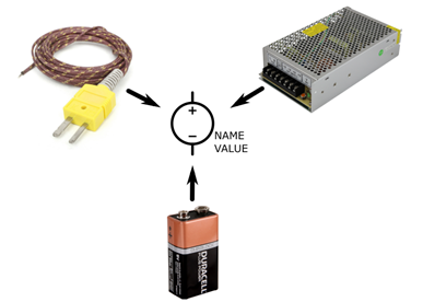
Figure 1: Real-life voltage supplies and the correspondent schematic symbol
Schematic Circuit Diagrams Symbols
Schematic circuit diagram symbols are the fundamental blocks of the design. Each component of the circuit is represented by at least one symbol, that characterizes an electrical functionality. Depending on the level of detail that the schematic needs to convey, one component can be represented by several of symbols: for example, a wire wound resistor can be described by a single resistance symbol in parallel with an inductor to represent the parasitic inductance. Figure 2 shows typical symbols for electronic components, using the US standard. As exemplified in the resistor section of Figure 2, that are two main standards for circuit schematics: the US and the British standards. The image shows only the US standard for most components.
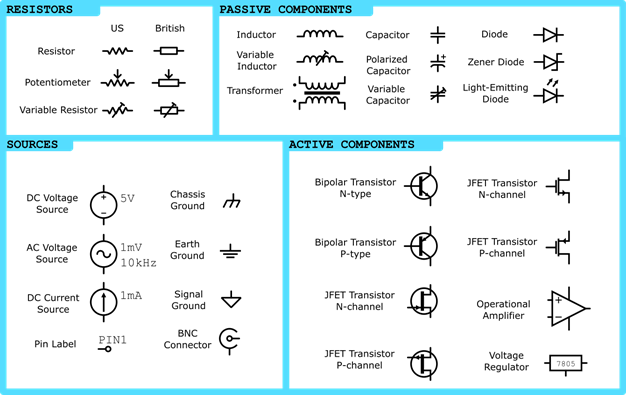
Figure 2: Schematic symbols for electronics
Resistors, inductors, capacitors, and diodes are represented by simple two-pin devices, whereas amplifiers and transistor symbols are more sophisticated. Also, depending on the nature of the electrical device, the symbol may present variations from the simple ones. For instance: variable passive components (such as variable resistors and capacitors) present a diagonal arrow overlapped to indicate variability, light-emitter diodes (LED) have two arrows pointing outwards to represent light, and Metal-Oxide-Silicon Field Effect Transistors (MOSFET) have different symbols than bipolar-junction transistors.
Besides component symbols, node labels are also used to identify interconnections and power supply. For instance, power labels are characterized by a name and/or a value: VCC = 5 V represents that the nodes are connected to external power supplies and PIN1 represents that the node is connected to a pin named PIN1. Power symbols and node labels can be used to facilitate readability and to specify the type of node (POWER, PIN, GND) to the layout editor.
A value and a unique reference name should be attributed to each component symbol. For instance, a resistor should be followed by a reference name and a value such as “R3 = 10 kΩ”. Active components and integrated circuits may be reference to a name and the code of the component model, such as ”U2 = AD825”. Name and value attribution are fundamental for readability. The industry standard for reference names, also called “Reference Designators”, defines unique letters for each component type:

Design Tools for Schematic Diagrams
During the design flow, electronics engineers can use simple hand drawn schematics to create new circuits and to perform quick calculations. However, software schematic tools are needed in professional projects for adequate documentation, simulation, and layout. Figure 3 present a short list of some design tools for electronic schematics.
Some tools are focused only on the schematics and are usually used for documentation purposes. The main advantage is that these tools are usually free and often online, without the need of downloading the software to start drawing. Also, because it is focused on the schematic documentation, the aesthetics of the symbols are usually more friendly. Tools that fall in this category : Scheme-It, CircuitLab and EasyEDA.
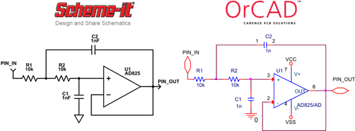
Figure 3: Sallen-Key filter drawn using Scheme-It and ORCAD Capture
However, professional tools typically provide features in addition to basic schematics. In fact, the schematic editor is usually only a stage of the complete design tool. The advantage of these programs is the capability of automatically simulate the circuit from the schematic, and using the connection and component information to feed the layout editor. Some of the most popular tools are ORCAD™ Capture, LTSpice™ Schematic Editor, KiCAD™ Schematic Editor, Altium™ Schematic Editor and TINA-TI™ Simulation Tool.
Sub-circuits and Component Design
Sub-circuits are fundamental tools to improve the organization and readability of a design. Complex schematics, with large component and interconnection count, often implement identical blocks of circuit that are repeated through the design. In these cases, representing the circuit by a single component may significantly clean the schematic. Tools that are used for simulation and layout typically provide the option of creating sub-circuits. When applying this feature, the designer should be aware of the file structure, as sub-circuits can be either designed as a schematic inside a bigger project or as a library file, that can be accessed by different projects. Also, the designer should create a new component symbol for the sub-circuit, with the design tool, assigning each external pin to the correspondent internal node.
Difference Between Schematic and Layout
Newbie designers can sometimes confuse schematic and layout drawings. However, they are fundamentally different: schematics are functional representations of electronic circuits, specifying only the type of components, their distribution, and interconnections. The layout, on the other hand, describes the physical interconnection between the components and specifies the design rules, such as path width, spacing, via size, layers, and packages. Schematic conceptualization is the first stage of the design flow, whereas the layout design is the last.
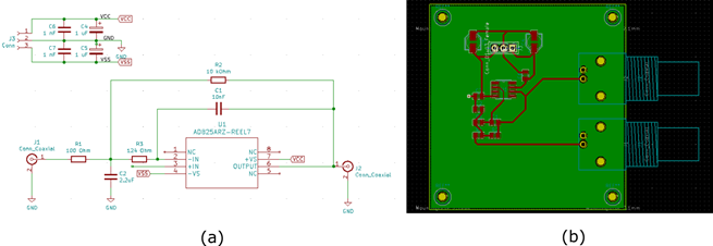
Figure 4: Schematic (a) and the correspondent layout (b) of a filter designed using KiCAD
Although very different, schematics and layout are intimately connected: the schematics are used in design tools to generate a netlist for the layout editor, using this information to check if the layout matches the circuit and to automatically distribute the components and route the paths using “auto place” “auto route” tools. Thus, schematics and layouts walk side-by-side during the design flow.
Schematics for Simulation vs Schematics for Layout
As we discussed previously, schematic diagrams is the first step to perform simulations and layout. However, there are some differences between a schematic for simulation and a schematic for layout. The first difference is the presence of stimulation signals. To simulate a circuit, at least one signal should be provided to the circuit. The most basic stimulation is the power voltage. In simulators such as PSPICE and LTSPICE, the power supply is typically represented by DC or AC voltage symbols (with name and value). Also, most simulations need input signals, which may be voltage or current symbols with different characteristics, such as waveshape, amplitude, frequency, etc.
On the other hand, input signals and supply voltage symbols are not presented in layout schematics. This is because, in the real circuit, these signals are interfaced with the board using connectors. Therefore, connector symbols (pin-headers, BNC, etc.) are used instead of voltage sources. These symbols contain the connector nodes, reference name and model, as shown by the J3 connector in Figure 5. Besides connectors, the layout schematic should also contain package symbols instead of simulation symbols for integrated components. The package symbol contains all the non-connected, digital, trimming and heat-sinking pins, which may not be available in the simulation symbol. Also, some packages contain two or more integrated circuit, that is often not available in simulation symbols.
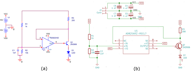
Figure 5: Schematic of a constant current source driving a LED on (a) ORCAD Capture for simulation and (b) KiCAD for layout
Finally, for simplification purposes, simulation schematics may neglect some components of the circuit, such as bypass capacitors and line-filters, which is the case of Figure 5. Also, some passive components are made of more than one device, such as parallel capacitors and resistors, to achieve non-commercial values. Although this is not problematic for simulations, the designer should adapt the schematic to apply in the layout editor. The layout schematic should contain all the components and connections used in the real circuit.
Tips and Tricks
Complex schematics are sometimes challenging to read, even for well-trained engineers. Knowing the symbol shapes and variations is often not enough to properly read a schematic. In fact, the main difficulty relies on identifying circuit blocks and understanding how the components are interconnected. If the design is well organized, each circuit block will be labeled with its name and function. When reading a new schematic, begin searching for the input blocks, containing the circuit inputs, and follow the signal flow until you find the output blocks.
The connection between components is usually made with net wires and labels. Wires should connect components close to each other, but as the number of components scales up, the use of wires becomes problematic. Figure 6 shows how the use of labels and net names can simplify a schematic and make it more readable. Pin labels should be used to connect different circuit blocks. This allows the use of different schematic pages for each block, improving organization and readability.
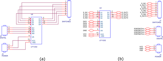
Figure 6: Confuse schematic using only wires (a) and cleaner schematic using labels (b)


