
Understanding FPGA Synthesis
06/08/2019, hardwarebee
Today, the process of FPGA synthesis plays a very integral and crucial role in the creation of FPGAs — ensuring that they work optimally and with high efficiency. FPGA synthesis, as suggested by the name, is a process of converting high level FPGA logic design into gates.
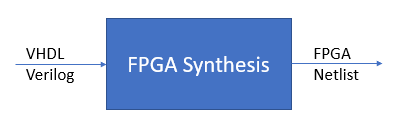
During the FPGA synthesis process, a high description design or an HDL design is converted into a gate level representation or a logic component. This means that FPGA code provided in high level language such as VHDL or Verilog is converted into logic gates using a synthesis tool.
A synthesis tool is a computer program that takes in instructions in the form of hardware description languages as input and generates a synthesized netlist as an output.
Synthesis tools typically generate netlist file and a bitsteam for FPGA code upload.
When formulating the logic and circuit design, Boolean algebra is used, including logic operations such as AND, OR, XOR, and NAND, operations. Synthesis tools then interpret this language into implementations for FPGAs (or ASICs). For FPGAs, look up tables, flip flops, and RAM blocks are employed whereas standard cell gates, flip flop libraries, and memory blocks are used for ASICs. In software engineers language, a FPGA synthesis tool is similar in functionality to a compiler.
FPGA Synthesis Benefits
The automation of the logic design and logic synthesis processes has produced a lot of convenience in the world of electronic design. To begin with, logic design in high level programming languages as well as using synthesis tools to generate logic gates, allows to be a certain level of standardization across the board between various designers and electronics manufacturers.
It also reduces the potential for errors and mistakes as well as allows us to reuse designs and modify them for future applications. Logic synthesis takes up a lot of responsibility from your shoulders onto its own, looking after the minute details to ensure that the entire process is as productive as possible while facing minimum roadblocks and bugs. The ability to reuse design means that there is a design that has been implemented onto an FPGA chip, it can later be implemented as an ASIC if needed for a different system at a different point in time.
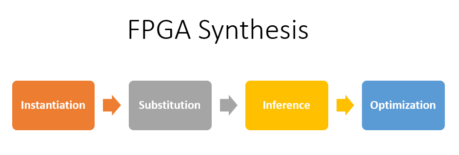
4 Steps of FPGA Synthesis
Instantiation
This is where the tool maintains a library consisting of primitive modules such as Boolean functions including AND, OR, NOR, etc., and other modules that have been defined by the user.
Substitution
This further expands into the primitive modules by adding language operators and constructors.
Inference
This is where the tool detects and recognizes particular patterns in the Verilog logic design or description and treats them in particular, user defined manner.
Logic Optimization
Here, the Boolean operations are grouped together in various combinations using logic minimization techniques.
List of FPGA Synthesis Tools
The following list comprises or FPGA synthesis software tool available in the market:
- XST (delivered within ISE) by Xilinx
- Vivado by Xilinx
- Quartus II integrated Synthesis by Altera
- IspLever by Lattice Semiconductor
- Encounter RTL Compiler by Cadence Design Systems
- LeonardoSpectrum and Precision (RTL / Physical) by Mentor Graphics
- Synplify (PRO / Premier) by Synopsys
- BlastFPGA by Magma Design Automation


