This website uses cookies so that we can provide you with the best user experience possible. Cookie information is stored in your browser and performs functions such as recognising you when you return to our website and helping our team to understand which sections of the website you find most interesting and useful.
Why crosstalk matters in PCB Design
06/08/2019, hardwarebee
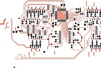
Traces on a printed circuit board (PCB) that are routed close together will interfere with each other. Virtually any trace on a PCB interferes with any other trace, but often at a level that we can neglect. We call this crosstalk. Depending on the spatial relationship between traces, they have a coupling inductance and a coupling capacitance. So any trace on a PCB can act as an “aggressor” signal to other “victim” signals.
In the general case, analysis software can consider any amount of trace segments coupling with each other. For sake of simplicity, in following pictures, we consider only two traces routed in parallel. Traces routed in parallel will form a “coupling capacitance” and a “coupling inductance”. Both of which will depend
- distance of the traces and dielectric environment
- length/distance at which traces are routed
- the closer together, the longer in parallel, the more coupling
Fieldsolver tools will help us to understand the details and create needfull parameters for simulation.
The strength of crosstalk (signal amplitude of crosstalk noise) is dependent on
- the closer traces come together, the longer that they are routed in parallel -> ++ crosstalk
- the more coupling -> ++ crosstalk
- the more dV/dt of the aggressor signal, i.e. the faster rise/fall time -> ++ crosstalk
Please note, that amplitude of crosstalk depends also on rise/fall times of aggressor signals. Which means, the same PCB layout might perform better or worse, when you changes the ICs or on programmable pins, change the slew rate/drive strength of IC pins.
How can crosstalk harm our signal?
Obviously, an aggressor could impose a disturbing voltage-level onto a victim signal. Like an aggressive digital signal, imposing noise on a sensitive analog signal. Likewise, a “slower” but high-voltage signal, can cause significant crosstalk into any other signal.
But often, the level of crosstalk noise will have a more non obvious impact.
It changes the timing of our signals!
“Timing of a signal” is always measured from a reference point, like when a signal crosses a certain voltage level. If crosstalk noise slightly impacts the voltage levels of our victim signals, obviously they will reach sooner or later those thresholds, hence appear “slower” or “faster” in relation to a clock signal for example. This can change setup/hold requirements significantly!
In order to analyze what can happen, we can extract from PCB-layout design or create by manual drawing a simulation setup reflecting two traces routed 4cm in total, but 2cm are routed in close distance and in parallel (trace width = 130um, trace-2-trace gap = 260um) so that they have relevant coupling. It is not needed to share more details than that for now.
Now let us do a simulation of both signals switching from low to high. We simulate without the coupling and we simulate in consideration of coupling. The green curve is the signal in isolation, the blue curve is the signal in consideration of coupling.
We observe, that a VinH level at 1.7V is reached later in time. Actually 7ps later. Now there is a rule of thumb, that with typical PCB material, we have about 15cm/ns (169ps/inch). Which means our 7ps are equivalent to 1mm of trace length! “One Millimeter”. Think about it. Often we specify length matching to require 100um or 0.5mm that all traces should have same length and if we do now a mistake in the design and have such an amount of crosstalk.
Think further to a bus routing, we have several signal going for longer distance in parallel and in worst case scenario, this amount of crosstalk to any victim can be even more and the impact on timing even worse.
When you are doing designs like with DDR memories. You might what to use a Signal Integrity tool to make this sort of analysis. There are several such tools in the market!
I am used to work with HyperLynx from Mentor a SIEMENS Business. It makes the extraction of PCB-Layout data very easy and gives me a “DDRx-Wizard” to validate DDRx memory interfaces. I will talk in another article why you should use such software tools to validate DDRx-Designs. Because DDRx signals are different. It is not only that DDRx signals need to reach a certain threshold, they need to follow a much more complex condition around the threshold level. Stay tuned for that article.
___________________________________________________
This is a guest post by Hans Hartmann, Director Sales and Marketing at Zitzmann GmbH, Founder EDA4YOU Sales Rep, Founder DELBOtronik GmbH


