
Boost Converter Overview
06/06/2023, hardwarebee
A boost converter, is a versatile power electronics circuit that plays a pivotal role in a wide range of applications. From electric vehicles and renewable energy systems to portable electronics and medical devices, the boost converter enables efficient power transfer, allowing devices to operate at desired voltage levels while minimizing energy loss.
The fundamental principle behind a boost converter is its ability to store energy in an inductor during one phase of an electrical cycle and then transfer it to an output capacitor during another phase. By utilizing a switching element, such as a transistor or a MOSFET, the boost converter regulates the flow of energy, resulting in a higher output voltage compared to the input voltage. This step-up process ensures that devices receive sufficient voltage levels for optimal performance, even when faced with low-input voltage scenarios.
One of the key advantages of a boost converter lies in its ability to provide voltage regulation, making it an essential component in portable electronic devices. By efficiently stepping up battery voltages, boost converters ensure that these devices can operate reliably across a wide range of input conditions, maximizing battery life and enhancing user experience.
Furthermore, the boost converter finds its application in the field of renewable energy. As solar panels or wind turbines generate low-voltage outputs, boost converters play a crucial role in stepping up the voltage to levels suitable for grid integration or battery charging. By effectively harnessing and transforming renewable energy sources, boost converters contribute significantly to the sustainable energy ecosystem.
In this article, we will delve deeper into the inner workings of boost converters, exploring their operating principles, key components, and design considerations. We will examine their role in various applications and shed light on the factors influencing their efficiency and performance. By understanding the intricacies of boost converters, engineers, researchers, and enthusiasts can unlock new possibilities in power management, paving the way for enhanced energy utilization and technological advancements.
So, join us on this enlightening journey as we unravel the secrets behind boost converters and discover their transformative impact on power conversion and efficiency.
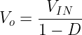
A Boost Converter is a type of DC-to-DC converter that it’s output voltage is higher than the input voltage. In an ideal converter, which is assumed to be lossless, power conservation is crucial. The output voltage is greater than the input voltage, but the input current is higher than the output current. The boost converter is characterized by the following equation:
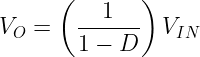
The relationship between input and output is given by the following equation:
![]()
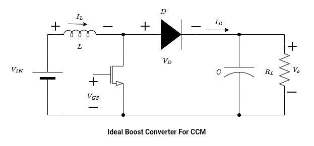
Let’s have a look at the circuit diagram, it is quite simple and consists of only a few components. It consists of an inductor, a power MOSFET for high-frequency switching, a freewheeling diode D, a capacitor C that serves as a filter, and a load resistor RL.
The MOSFET works as a switching element.
The boost converter is toggled on and off using Pulse Width Modulation (PWM) techniques. PWM can be implemented either based on time or frequency. Time-based modulation is commonly employed in Boost Converters due to its simplicity in construction and operation.
The switching frequency is given by,
![]()
There are two modes of operation in a boost converter:
- Continuous Conduction Mode (CCM)
- Discontinuous Conduction Mode (DCM)
Continuous Conduction Mode (CCM)
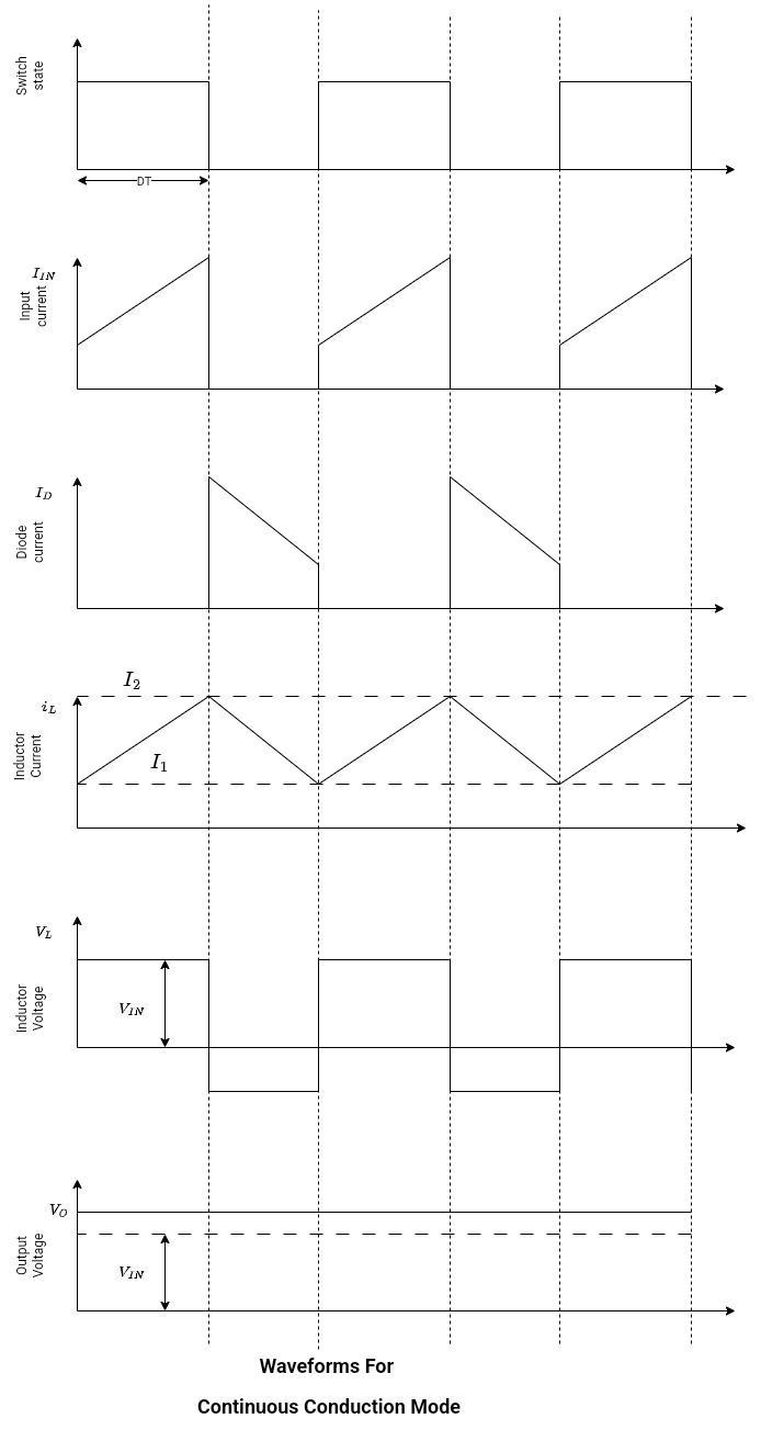
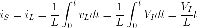
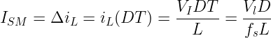
In this mode, the inductor current iL flows continuously during the entire switching cycle and hence never reaches zero. In other words, the MOSFET turns off to turn on again before the inductor is completely discharged. The switch duty cycle in CCM is given as
![]()
In this mode, two intervals in each switching cycle are charge and transfer.
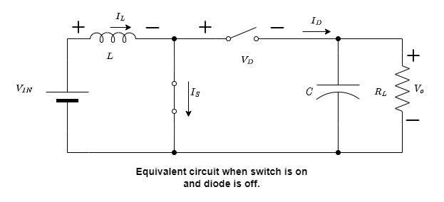
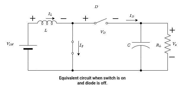
On State: The switch is on at 0 < t ≤ DT. The equivalent circuit for the ‘on’ state is given below.
During the ‘on’ state of the switch, the voltage across the diode is given by:
![]()
Hence, the diode is reversed-biased. The voltage across the inductor is given by:
![]()
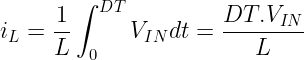
The inductor current rises linearly from I1 to I2 with a slope of VIN/L. The current flows through the inductor in a clockwise direction. The inductor stores energy by generating magnetic fields. It charges up to the VIN. The left side of the inductor is positive, as shown in the schematic diagram below. The current path is also given; it flows to the transistor Q1 and is then grounded. The voltage across the inductor remains the same throughout this interval; hence, it charges linearly. The maximum inductor current at the end of the ‘on’ state is given by:
The duration of the ‘ON’ state can be found by using the expression below:
![]()
At time t = DT, the switch turns off.
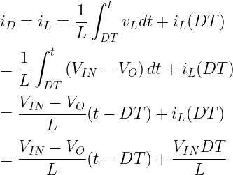
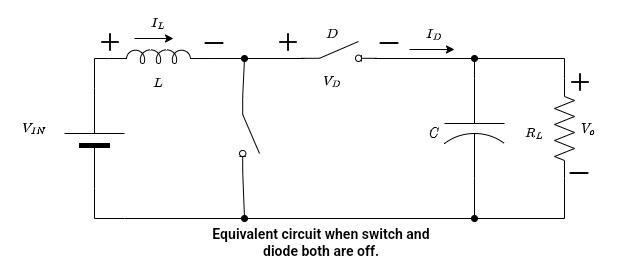
Off State: The switch is off at t = DT. The equivalent circuit for the ‘off’ state is given below:
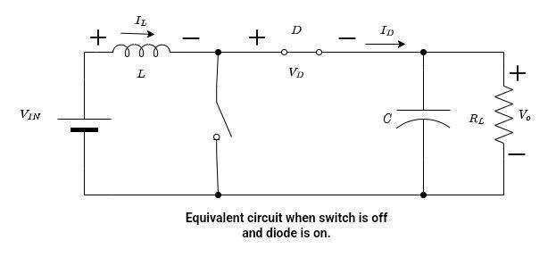
The inductor current cannot vary abruptly. Therefore, the polarity of the inductor reverses to preserve the inductance. The left side of the inductor is negative. The inductor voltage is given as
![]()
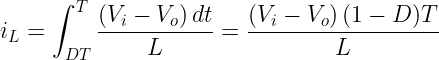
It will turn on the freewheeling diode. Because there is stored energy in the inductor, it will act as a current source. The inductor current starts to decrease linearly from I2 to I1 with a slope of The inductor current is given by the following equation.
During this interval, the energy stored in the inductor along with the input voltage source is transferred to the load resistor RL and charges the capacitor C as well.
The duration of the ‘off’ state is given by the following relationship:
![]()
The output voltage is given as:
At the time t = T, the switch turns on again.
Assume that if the turn-on time of the transistor Q1 is greater than the turn-off time, then the inductor charges for a longer time.
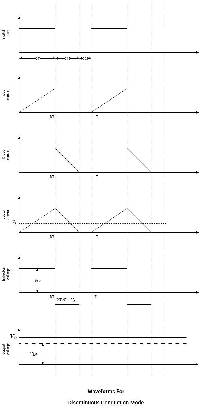
Discontinuous Conduction Mode (DCM)

In this mode, the inductor current iL falls to zero during a portion of each switching cycle. The switching cycle is composed of three intervals: charge, transfer, and idle.
On State: This is the charging state and the inductor charges.
The switch is on at 0 < t ≤ DT. The input voltage is applied across the inductor (L) and the switch, causing the current to rise. During this interval, the switch is on and the diode is off. The voltage across the diode is
![]()
The voltage across the inductor is VIN and the inductor current increases linearly from 0. Energy is stored in the inductor during the ON time of the switch, reaching its maximum value at t = DT. The inductor current is equal to the switch current during this interval and is given as
Maximum switch and inductor current occurs at t = DT and is given below:
The duration of the ‘on’ state
![]()
The switch turns off at time t = DT.
Off State: During the interval DT< t ≤ (D+D1)T, the switch remains off.
The diode turns on, and hence vD = 0 and iS = 0. The inductor and diode currents are the same during this interval, as given by:
The peak diode current and inductor current are given as:
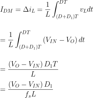
Idle State: During this interval (D+D1)T <t ≤ T, both diodes and switch are off.
The inductor current iL, switch current iS, and diode current iD is zero, as shown on the waveforms as well. The voltage across the switch is
vS = VIN
The voltage across the diode is:
VD = VIN – VO
The output voltage waveform in DCM experiences a ripple due to the intermittent nature of the inductor current. The equation for the output voltage in DCM can be expressed as:
The above equation shows the input and output relationships of the converter. The output voltage is always greater than the input voltage.
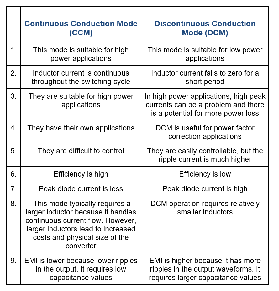
CCM vs DCM Comparison
Advantages
Boost converter is implemented with a minimum number of parts and has a relatively simple circuit design, making them cost-effective. The circuit is compact and suitable for portable applications. Boost converters.
It produces an output voltage that is higher than the applied input voltage. They are suitable for applications where voltage step-up conversions are required.
They provide high efficiency for a duty cycle of 0.5, hence minimizing power loss and maximizing energy conversion.
Boost converters offer excellent voltage regulation capabilities. They can produce stable output voltage levels regardless of fluctuations in the input voltage or load variations.
Disadvantages
The output current of the circuit is pulsating, hence a larger capacitor is required to reduce ripples.
It may introduce electromagnetic interference (EMI) issues. Due to the rapid switching of currents, boost converters can produce EMI, needing additional EMI filtering methods for compliance with standards.
The boost converter has a poor ability to prevent hazardous transients and failures.
They have limited output current capacity, so their applications are limited to low to moderate output power applications.
The efficiency is poor if the duty cycle is very large or very small. Therefore, high gain operation cannot be achieved with this converter. Efficiency can be as poor as 60% for a duty cycle of 0.7 or 0.3. Whereas it has 90% efficiency for a duty cycle of 0.5.
Applications
Boost converters play a critical role in solar systems, particularly in photovoltaic applications. In solar arrays, there is a need for voltage boosters that are efficient in stepping up voltage, cost-effective, and compact. Since the input voltage from solar arrays fluctuates with weather conditions, boost converters are commonly used to step up the voltage to meet specific requirements in these systems.
Boost converters are extensively used in LED lighting systems, especially for driving multiple LEDs in series. This configuration ensures uniform current distribution and provides the required voltage levels. As a result, it promotes energy efficiency and achieves the desired brightness levels.
Boost converters have a major application in power factor correction (PFC) applications. PFC is the ratio of real power to apparent power, and it is used to enhance power in electrical systems. In these applications, boost converters regulate the input current and enable the system to draw current in a way that minimizes power losses associated with low power factor. This leads to improved system efficiency.
Boost converters are essential components in electric vehicle power systems. They increase the battery voltage to power various electrical components, such as meeting the higher voltage demands of the motor drive system, auxiliary systems, and charging infrastructure.


