
FPGA Image Processing: Ultimate Guide
27/03/2025, hardwarebee
As technology races forward, so does the demand for high-performance, efficient image processing solutions that can keep up. FPGAs, or Field Programmable Gate Arrays, have emerged as a versatile choice for such advanced processing tasks due to their unique blend of customizable hardware and impressive computing abilities. Understanding the intersection of FPGA technology and image processing not only empowers engineers but also pioneers new territories in embedded systems and real-time computational tasks.
At the heart of FPGA technology is a reconfigurable architecture, offering unparalleled flexibility in hardware design. With foundational elements such as Configurable Logic Blocks, Programmable Interconnects, and robust I/O interfaces, FPGAs have evolved dramatically since their inception. Today, they drive innovative applications across industries, from aerospace to automotive, demonstrating their adaptability and diverse utility.
In this ultimate guide, we delve into the core components and architectural styles of FPGAs that set the stage for image processing. We explore their advantages, including flexibility and real-time processing prowess, and address the challenges faced in their implementation. Covering tools, software, and practical applications, this guide aims to illuminate the path for newcomers and seasoned professionals alike in the realm of FPGA image processing.
Introduction to FPGA Technology
Field-Programmable Gate Arrays (FPGAs) have revolutionized the way digital systems are designed and implemented. FPGAs are unique in their ability to be reconfigured after manufacturing. This reconfigurability makes them ideal for a wide range of applications. From digital signal processing to real-time applications, the versatility of FPGAs is unmatched. By using programmable logic devices, FPGAs offer solutions that meet the exact design and performance requirements of complex applications. Understanding FPGA technology can be transformative for anyone interested in digital designs. From development time to performance optimization, FPGAs offer numerous benefits that can address a wide variety of design requirements.
What is an FPGA?
An FPGA, or Field-Programmable Gate Array, is a special type of semiconductor device. Unlike traditional chips, FPGAs are highly versatile because they consist of programmable logic blocks. These blocks can be configured to perform different digital functions. Users can design FPGA-based systems by creating binary files that dictate how the device should operate. FPGAs also include programmable interconnects that help connect these logic cells together. This ability to rewire internal connections allows FPGAs to adapt to different tasks. The reconfigurable hardware of FPGAs makes them popular in a range of applications, from digital signal processing to implementing complex algorithms such as Neural Networks.
Key Architectural Components
The internal structure of FPGAs is composed of several fundamental components. At their core are Configurable Logic Blocks (CLBs), which serve as the building blocks for digital circuits. Each CLB can perform a specific logic function depending on the design needs. A wide range of functionality can be realized by organizing these blocks into larger, more complex designs. Beyond the CLBs, FPGAs also feature programmable interconnects. These interconnects are crucial for linking logic blocks and setting up paths for data flow.
Another important feature is Configuration Memory, which stores the current settings of the FPGA. As needs change, this memory can be updated to revise the functionality of the FPGA. Also, FPGAs can connect to external memory, which is beneficial for tasks requiring significant data storage, such as real-time image processing. With these components, FPGAs offer the flexibility to create custom digital systems tailored to specific tasks.
FPGA Evolution and Applications
Since their invention, FPGAs have continually evolved to meet increasing design and performance demands. Early models were simple, focusing mainly on basic logic functions. Over time, advancements in design tools and programming languages have made them accessible to a wider audience, even those with only a basic knowledge of hardware design. The development process for FPGAs has also become streamlined, reducing development time significantly.
FPGAs are now used in a diverse range of applications, from automotive systems to telecommunications. They are particularly valuable in real-time processing tasks, where speed and adaptability are critical. Today’s FPGAs are capable of handling complex designs and applications such as Neural Networks, providing a robust platform for digital innovation. As technology advances, FPGAs continue to be a key component in next-generation digital systems, offering unparalleled flexibility and power.
Understanding FPGA Architecture
Field-Programmable Gate Arrays (FPGAs) are versatile devices used in a wide range of applications. They are key in digital systems because they provide high performance and flexibility. FPGAs consist of a matrix of programmable logic, memory resources, and interconnected pathways. These elements allow FPGAs to meet varied design and performance requirements. By using design tools, engineers can configure an FPGA to execute complex designs rapidly. This architecture makes FPGAs ideal for real-time applications. Understanding each element of FPGA architecture helps in optimizing design, reducing development time, and improving efficiency.
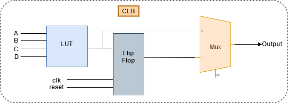
Configurable Logic Blocks (CLBs)
Configurable Logic Blocks (CLBs) are the core of an FPGA’s architecture. They contain logic cells that execute basic functions like AND, OR, and NOT operations. These logic cells combine to form complex applications. By using programmable logic, CLBs can be tailored to meet specific design requirements. This adaptability makes FPGAs valuable for a range of applications needing custom logic. Knowledge of hardware design is crucial to leverage the full potential of CLBs. As a result, engineers can build digital systems that align with precise performance requirements.
Programmable Interconnects
Programmable interconnects are vital for linking different components within an FPGA. They facilitate communication between logic blocks, memory resources, and external interfaces. This network of paths lets designers create custom connections that match their specific needs. Programmable interconnects enhance the flexibility of digital designs, allowing for rapid adjustments during the development process. They ensure that data flows efficiently across the FPGA, reducing latency in digital signal processing tasks. Proper configuration of these interconnects is crucial to minimizing development time and ensuring optimal performance.
Memory Resources and I/O Interfaces
Memory resources in FPGAs support a range of applications by storing configuration data and intermediate processing results. They include blocks of Configuration Memory and external memory options to accommodate different data needs. I/O interfaces in FPGAs allow these devices to connect with external systems, facilitating data exchange. These interfaces can be configured to handle multiple types of digital signals. By using these resources efficiently, developers can create digital designs that balance speed and functionality. Understanding their roles ensures that FPGAs can meet the rigorous demands of complex designs, including those in real-time and neural network applications.
FPGA Architecture Styles
Field-Programmable Gate Arrays (FPGAs) offer a variety of architecture styles to meet diverse design requirements. Each style plays a crucial role in how the FPGA performs in different applications. An FPGA’s internal configuration can drastically affect its ability to handle complex designs and ensure efficient operation for a range of applications. Understanding these architecture styles is essential for anyone involved in digital designs and seeking to optimize performance in real-time applications. FPGAs’ reconfigurable hardware provides the flexibility needed for specialized knowledge applications, making them ideal for both simple and complex applications.
Symmetrical Array Architecture
Symmetrical Array Architecture is one of the most common styles in FPGA design. This architecture features a grid-like pattern of configurable logic blocks. These blocks are connected by a programmable interconnect, enabling a wide range of digital systems. The design’s uniform structure simplifies the development process, making it faster and more efficient. The symmetrical layout also allows for easy scalability, which can be adapted to various performance requirements. This style is widely used in many digital signal processing tasks and is suitable for applications needing high throughput.
Row-Based Architecture
Row-Based Architecture organizes its configurable logic blocks in horizontal rows. Between these rows lie channels that serve as programmable interconnects. This setup allows data to flow smoothly from one end of the array to the other. The design promotes efficient use of FPGA resources by optimizing connectivity paths. It is particularly effective in handling sequential processing tasks and is often used when performance requirements dictate a linear data flow. This architecture can be especially beneficial for real-time applications, where minimizing development time is crucial. As such, it finds its place in applications ranging from simple automation to more advanced neural networks.
Digital Signal Processing Blocks
Digital Signal Processing Blocks (DSPs) are specialized elements within an FPGA focused on arithmetic operations. These blocks are vital for tasks such as filtering, modulation, and other signal processing applications. DSPs enhance an FPGA’s capability to manage complex numerical tasks quickly and efficiently. By integrating DSPs, designers can offload computationally intensive tasks from general-purpose logic cells, freeing up resources for other digital designs. This integration helps in managing external memory efficiently and allows rapid data processing. As such, DSP blocks are indispensable in applications requiring high-speed data manipulation and are key components in modern FPGA design flows.
Advantages of FPGAs in Image Processing
Field-Programmable Gate Arrays (FPGAs) offer a wide range of advantages for image processing. They are powerful tools for handling complex designs in digital systems. FPGAs provide the ability to meet specific performance requirements and design functions effectively. They are known for their versatile nature, enabling them to adapt to different design requirements. This adaptability makes them ideal for a variety of real-time applications, where speed and accuracy are crucial.
Flexibility and Scalability
One of the most significant benefits of FPGAs in image processing is their flexibility and scalability. FPGAs contain configurable logic blocks and programmable interconnects, allowing them to be tailored for specific tasks. This configurability offers more control over design functions than traditional processors. Engineers can reconfigure FPGAs to meet new challenges or improve existing processes. This flexibility also makes FPGAs a great choice for a wide range of applications—from simple tasks to complex designs.
Scalability is another advantage. FPGAs can grow with the demands of modern digital systems. As processing needs evolve, FPGAs can be upgraded or reprogrammed without needing entirely new hardware. This ensures that the FPGA design can efficiently scale with the project requirements.
Real-Time Processing Capabilities
FPGAs excel in real-time processing applications due to their parallel processing abilities. Unlike processors that handle tasks sequentially, FPGAs can process multiple data streams simultaneously. This capability is crucial in digital signal processing, where real-world data needs immediate analysis and action. Image processing demands quick handling of large volumes of data, making FPGAs an ideal tool to meet these performance requirements.
Real-time applications benefit from FPGAs’ low latency. The quick response time is vital for applications such as video surveillance and automotive safety systems. With FPGAs, complex applications can run efficiently, ensuring timely processing of data without delays.
Comparison with ASICs and PLDs
When compared to ASICs (Application-Specific Integrated Circuits) and PLDs (Programmable Logic Devices), FPGAs offer unique advantages. ASICs are crafted for specific tasks and provide high performance, but they lack flexibility. Any design changes require new production, leading to increased costs and development time.
PLDs provide some programmability but fall short of the complex and customizable designs possible with FPGAs. FPGAs’ reconfigurable hardware gives developers a significant edge in adapting designs without starting from scratch. Additionally, knowledge of hardware design is less intensive with FPGAs compared to ASICs, allowing for greater ease in the development process.
In summary, FPGAs stand out due to their versatility, upgradability, and performance in real-time applications, surpassing the static nature of ASICs and basic capabilities of PLDs.
Challenges in FPGA Image Processing
Field-Programmable Gate Arrays (FPGAs) are crucial in digital image processing. They enable customization for a wide range of applications such as real-time image processing and complex designs. Despite their potential, challenges in FPGA image processing include power management, design complexity, and cost concerns. Each area presents unique hurdles, affecting performance and development time. Recognizing these challenges can help manage design requirements and meet performance needs more effectively. This section will explore issues in power consumption, design and debugging, as well as cost considerations, providing insights into navigating the complexities of FPGA use in image processing.
Power Consumption and Management
Power management is a significant challenge in FPGA image processing projects. FPGAs offer flexibility due to their reconfigurable hardware, but this adaptability comes at a cost of increased power usage. The programmable logic and logic cells inside FPGAs can consume significant power, especially in complex applications. Managing power efficiently is essential to maintain system reliability and meet performance requirements. Careful planning during the design phase, including the choice of configuration memory and external memory, can help save power. Effective use of low-power design tools can also reduce consumption, but it requires specialized knowledge.
Complexity in Design and Debugging
Designing with FPGAs for image processing involves complex digital systems. The configurable logic block and programmable interconnect within FPGAs demand thorough understanding and precision. These elements make FPGAs adaptable to complex designs, but they also increase design complexity. Debugging these digital designs is another hurdle, requiring extensive knowledge of hardware design and logic functions. As these systems evolve, so do their design flows, making it crucial to keep up with advancements in design tools and techniques. Breaking down complex tasks into smaller, manageable parts can streamline the development process. However, it is often a time-consuming and specialized task.
Cost Considerations
The cost of FPGAs in image processing is a vital factor that can affect projects. While FPGAs allow for powerful and adaptable digital signal processing, they often come with high initial costs due to their complex nature and development process. These costs include hardware expenses and the time spent on design and debugging phases. External memory, configuration memory, and programmable logic devices contribute to the overall expense, especially in custom-field applications like neural networks. Balancing cost with performance and range of application needs is key. Careful planning and selection of FPGA features that align with specific design functions can ensure efficiency without compromising budgetary constraints.
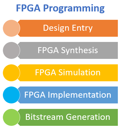
FPGA Development Process for Image Processing
Using Field-Programmable Gate Arrays (FPGAs) in image processing offers unparalleled flexibility and performance. FPGAs are versatile, allowing for real-time applications due to their high-speed processing capabilities. The development process for FPGA-based image processing involves several crucial steps, starting with understanding the design requirements. This ensures the creation of efficient digital systems. The process involves configuring logic cells and programmable logic blocks, which form the backbone of FPGA technology. The use of design tools to simulate and verify the digital designs is also vital. This guide aims to give a comprehensive overview of the process, from initial concept through to testing. With this knowledge, developers can create complex designs that meet specific application needs.
Design Workflow Overview
The design workflow for FPGA image processing begins with defining design functions that align with performance requirements. This step involves selecting suitable design flows and programmable interconnects for the project. Next, the development process requires design tools to simulate the digital signal processing. A thorough understanding of hardware design is crucial for configuring the Configurable Logic Block. The design workflow encompasses several iterations, allowing for adjustments to meet complex application demands. By utilizing external memory and configuration memory, FPGAs provide a wide range of applications. Each step in the workflow contributes to optimizing the performance and functionality of the final product, ensuring the solution meets real-time application needs.
RTL Simulation and Verification
Register Transfer Level (RTL) simulation and verification are critical components in FPGA image processing. The process begins by writing a hardware description language (HDL) code representing the digital designs. This code is then simulated to confirm that the design performs as intended. During simulation, developers can identify and correct errors, reducing development time. The verification step involves rigorous checking against design requirements, ensuring every function operates correctly within the system. With specialized knowledge, developers use simulation tools to improve complex designs, validating them before hardware implementation. This thorough approach ensures that potential issues are addressed early, saving time and resources in later stages.
Hardware Implementation and Testing
After successful simulation and verification, the next phase is hardware implementation. This involves loading the binary files onto the FPGA, configuring the programmable logic, and setting up programmable logic devices. The implementation step transforms the verified design into a functioning system using reconfigurable hardware. Once the FPGA is programmed, testing ensures it meets all performance specifications and is ready for real-time applications. Testing involves verifying the accuracy of outputs and fine-tuning hardware to handle the image processing tasks efficiently. With the help of design tools, developers monitor performance in various scenarios, ensuring reliability and prompt response of digital systems. This final stage is crucial for delivering a robust and efficient solution.
Tools and Software for FPGA Design
Designing with Field-Programmable Gate Arrays (FPGAs) requires specific tools and software tailored to handle complex digital systems. To meet the design requirements, engineers employ design tools that facilitate the creation and testing of digital designs. These tools help in managing programmable logic blocks, offering a range of applications from simple designs to complex applications. With a focus on configurable logic blocks and programmable interconnect, these tools ensure that the design functions align with performance requirements. Specialized knowledge of hardware design can also enhance the development process, reducing development time. Tools and software for FPGA design vary widely, accommodating both beginners and experts in creating digital signal processing systems.
Xilinx and Altera Tools
Xilinx and Altera provide popular tools for FPGA design. Xilinx offers the Vivado Design Suite, a comprehensive toolset for designing complex digital systems. It supports reconfigurable hardware and includes programmable logic for creating logic cells. Using Vivado, engineers can handle a wide range of digital designs through an intuitive interface that reduces development time. Similarly, Altera, now part of Intel, provides the Quartus Prime software suite. Quartus Prime helps in the design and integration of FPGA systems. It offers efficient design flows and configuration management for logic blocks. Both Xilinx and Altera tools are instrumental in real-time applications and can interface with Configuration Memory for flexible design adaptation.
OpenCV Integration for Image Processing
OpenCV is a powerful library used in image processing applications. Integrating OpenCV with FPGA platforms combines the flexibility of software with the speed of hardware. This integration allows the handling of complex designs that involve digital signal processing. By using OpenCV, FPGAs can process video and images in real time, extending the range of applications. This is particularly useful for Neural Network implementations, where fast and efficient data processing is crucial. Developers can use OpenCV to develop binary files that FPGAs can execute. This combination facilitates the design tools’ capability to interface with external memory while managing image processing tasks.
Interfacing with Image Sensors
Interfacing FPGAs with image sensors is essential for real-time applications requiring digital imaging. This process involves connecting digital designs with image sensors to capture and process visual data. FPGAs offer programmable interconnects that easily interface with these sensors. As image sensors capture data, FPGAs process it through programmable logic devices. This system ensures high-performance requirements are met, as it enables quick response times and efficient data handling. With reconfigurable hardware capabilities, FPGAs manage a range of applications by adapting to varying design requirements. The development process benefits by reducing time and complexity, providing a seamless integration with image sensors.
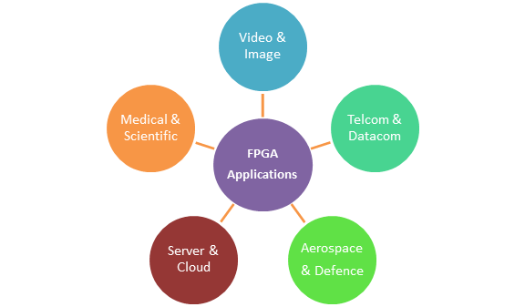
Practical Applications of FPGA Image Processing
Field-Programmable Gate Arrays (FPGAs) are powerful tools in image processing. They use programmable logic to handle complex designs and offer a wide range of applications. FPGAs excel in real-time applications where speed is crucial. Thanks to Configurable Logic Blocks, they can process data faster, meeting tight performance requirements.
These devices shine in digital signal processing and digital systems. They use logical cells and programmable interconnects to adapt to specific tasks. For image processing, they transform digital data into clear images effectively. With external memory, FPGAs manage large datasets during processing.
FPGAs suit applications with unique design requirements. They’re great for Neural Networks, where reconfigurable hardware offers flexibility. However, working with them requires specialized knowledge and design tools. Understanding design flows is crucial for transforming binary files into practical solutions.
FPGA Image Processing Applications:
- Real-time video encoding/decoding
- Medical imaging systems
- Surveillance cameras
- Industrial inspection systems
Using FPGAs in image processing can shorten development time. They provide a balance of speed and flexibility, making them ideal for complex applications. With the right design tools, FPGAs can improve the performance of digital designs significantly.


