
Understanding Charge Pump
29/12/2022, hardwarebee
Introduction
A charge pump is a type of electronic circuit that is used to increase the voltage of a DC power supply. It works by using a series of switching elements, such as transistors or diodes, to transfer charge from one storage element to another, resulting in a higher voltage output. Charge pumps are often used in portable electronic devices, where the limited space and power availability make it difficult to use a traditional transformer-based voltage boost circuit. They are also used in other applications where a high voltage is required, such as in automotive systems and in some types of LED lighting. In this article, we will delve into the operation and design of charge pumps, as well as the advantages and limitations of this type of voltage booster.
The concept of the charge pump dates back to the early days of electronic circuit design, with the first recorded patent for a charge pump circuit being issued in 1936. However, it was not until the development of more advanced switching elements, such as MOSFETs and CMOS technology, that charge pumps became widely used in practical electronic circuits.
One of the earliest and most well-known applications of the charge pump was in the design of the IBM PC/AT keyboard, which used a charge pump circuit to boost the voltage of the 5V DC supply to the high voltage levels required for driving the keyboard’s electromagnetic coils. This allowed for a compact and efficient design, as it eliminated the need for a large transformer.
Since then, charge pumps have been used in a variety of electronic devices and systems, including cell phones, portable music players, laptops, and other portable electronic devices that require a high voltage boost in a small package. They have also been used in automotive systems, such as in fuel injectors and ignition systems, and in LED lighting systems.
Positive Charge Pump Principles
Generally, capacitors are energy-storage elements that are charged by a DC voltage source like a battery. Therefore, two or more charged capacitors can be connected in series to build a higher voltage in the output. However, this way of increasing voltage is not useful because capacitors immediately must be charged when they discharge to a load. To enhance the circuit, a capacitor and a diode can be connected, as shown in Figure 1. In this circuit, a diode is in series with the DC voltage source and is parallel to a capacitor. The capacitor is also connected to a square-wave voltage source, oscillating between zero and Vdc. At first, the square-wave voltage is zero, and the diode is on. Thus, the capacitor gets charged to reach Vdc. Then, the square-wave voltage is equal to Vdc, and the diode is off because the cathode voltage is greater than the anode one. Therefore, the output voltage would be the sum of the oscillating voltage and the capacitor voltage, which is 2Vdc.
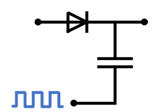
Figure 1: A basic circuit for increasing the DC input voltage
However, when the square-wave voltage falls to zero, the output voltage backs to Vdc, which is undesirable. For instance, if there is a 9V DC voltage source, and the square-wave peak voltage is also 9V, the output voltage will fluctuate between 9 and 18V.
To solve this problem in the presented circuit, a diode and a capacitor can be added to the circuit output to build up a constant voltage, as shown in Figure 2. In this circuit, the DC voltage source charges both capacitors to Vdc at first (when the square-wave voltage is zero). Then, the voltage across the first capacitor will rise to 2Vdc, when the square-wave voltage is at its peak value. In this case, the second capacitor will be charged to 2Vdc, meaning the voltage across both capacitors are the same. At this time, the output voltage remains at 2Vdc, even though the square-wave voltage is zero, because the voltage across the second capacitor is 2Vdc, the current cannot flow back due to the presence of a diode. Since this circuit can double the input voltage, it is called a voltage-doubler or charge pump.
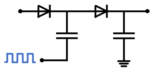
Figure 2: Stabilized doubled input voltage using two diodes and two capacitors
In reality, diodes are not ideal, and a voltage drop must be considered for them. Generally, the voltage drop for silicon-based diodes is between 0.6 and 0.7V. Although the mentioned voltage is small, it can affect the output voltage magnitude. Thus, the modified output voltage considering the diode voltage drop will be 2Vdc-2Vd. It means that, in the mentioned example, the output voltage must be modified to 18-2×0.6=16.8 V. Moreover, in loading conditions, the load current discharges the capacitor and produces small ripples in the output voltage. However, if the current is low enough, the described voltage can be obtained.
Adding another stage to previous circuit, the input voltage can be tripled. For this purpose, a diode and capacitor set must be added between the existing sets. However, the square-wave signal must be inverted, as shown in Figure 3. The NOT gate, which is in series with the second capacitor inverses the square-wave signal. The principle is as same as the voltage-doubler circuit. In fact, when the voltage across the second capacitor reaches 2Vdc, the inversed square-wave voltage will shift up the voltage across the third capacitor to 3Vdc. The rest is the same, meaning that the diode voltage drops reduce the output voltage, and the load current can produce ripples on the output voltage.
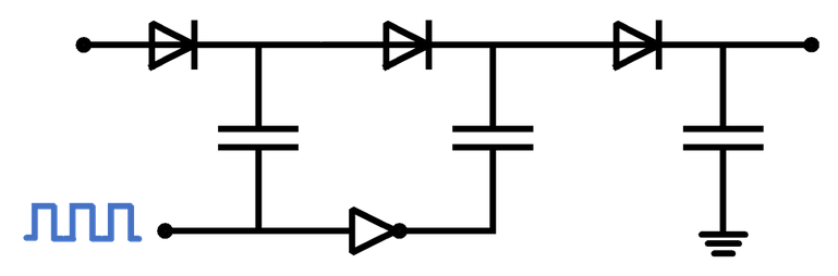
Figure 3: Positive charge pump circuit for tripling the input voltage
These circuits described positive charge pumps that provide positive voltage at the output. In the following section, the negative charge pump circuits will be discussed, and various configurations will be presented that produce negative output voltages.
Negative Charge Pump Principles
The circuit for producing negative voltage is quite different, as the diode and capacitor locations are not as same as the positive charge pump. As can be seen in Figure 4, the diode is connected to the ground, and the output voltage is the voltage across the diode, while the output voltage is the voltage across the capacitor in the positive charge pump. When the input voltage is zero, the output voltage is also zero, and the diode is off. When the input voltage reaches its peak, the diode is turned on, but the output voltage is still zero because the diode short-circuits the output. When the voltage goes back to zero, the diode gets off, and the input voltage is subtracted from the zero voltage across the output. Thus, the output voltage will be –Vdc. However, the output voltage is not constant and oscillates between zero and –Vdc. To have a nice DC voltage at the output, another set of diode and capacitor must be added to the circuit.
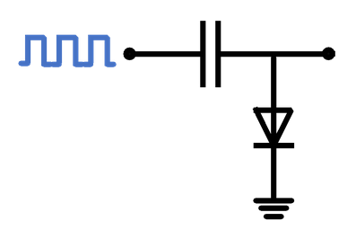
Figure 4: A basic circuit for decreasing the input voltage
Figure 5 shows a negative voltage doubler circuit with two diodes, two capacitors, and one oscillating input voltage. To stable the output voltage, the second capacitor is charged to –Vdc. Therefore, the output voltage is still –Vdc while the oscillating voltage falls to zero.
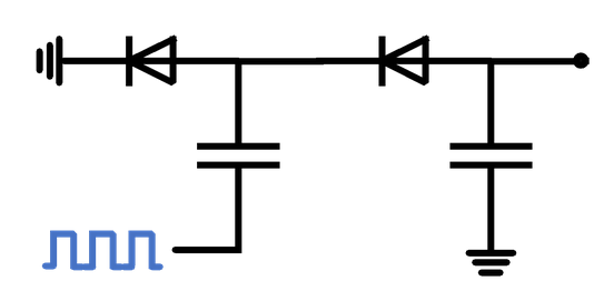
Figure 5: Stabilized negative voltage using two diodes, two capacitors, and an oscillating input voltage
The circuit can be improved to create the double negative voltage (-2Vdc), as shown in Figure 6. In this case, an inversed oscillating voltage must be connected to the second stage to shift down the voltage. For example, if the input voltage oscillates between zero and 9, the output voltage will be -18. It also should be noted that the diodes are not ideal in the real world, and the drop must be considered in the design stage. Furthermore, the load current can create ripples in the output voltage.
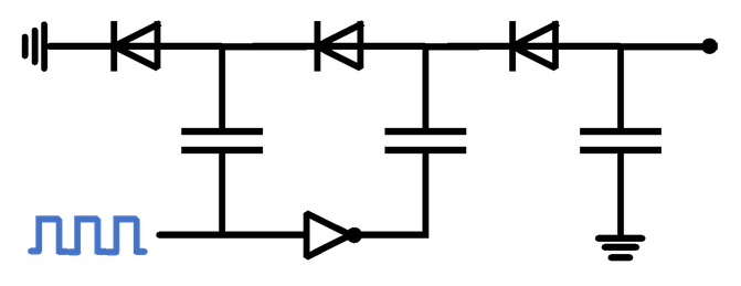
Figure 6: Negative voltage-doubler circuit
Charge Pump Design Tips
- Determine the required output voltage: The first step in designing a charge pump circuit is to determine the desired output voltage. This will depend on the specific application and the requirements of the load. It is important to keep in mind that the output voltage of a charge pump will typically be lower than the input voltage, due to losses in the switching elements and other circuit components.
- Select the appropriate switching element: The choice of switching element will depend on the required output voltage, the input voltage, and the current requirements of the load. Common options include diodes, MOSFETs, and CMOS inverters.
- Consider the switching frequency: The switching frequency of a charge pump circuit should be chosen based on the requirements of the application and the capabilities of the switching elements. Higher switching frequencies can result in higher output voltage, but also result in higher power consumption and increased switching losses.
- Size the storage capacitors appropriately: The storage capacitors in a charge pump circuit play a critical role in determining the output voltage and current capabilities. They should be sized appropriately based on the required output voltage and current, as well as the switching frequency and the input voltage.
- Use a good-quality input filter: A good-quality input filter can help to reduce the noise and ripple on the input voltage, which can improve the performance and stability of the charge pump circuit.
- Use a low-ESR output filter: The output filter should be designed with low equivalent series resistance (ESR) to minimize losses and improve the efficiency of the charge pump circuit.
- Use a good-quality bypass capacitor: A bypass capacitor can help to reduce noise and improve the stability of the charge pump circuit.
- Use a suitable control scheme: The choice of control scheme will depend on the specific requirements of the application and the complexity of the circuit. Options include pulse-width modulation (PWM) control and on/off control.
- Consider the power efficiency: The power efficiency of a charge pump circuit should be considered in the design process, as it will affect the overall performance and battery life of the device.
- Test and verify the design: It is important to thoroughly test and verify the performance of the charge pump circuit to ensure that it meets the requirements of the application. This may include testing under different load conditions and at different input and output voltage levels.
Charge Pump Applications
As mentioned in this article, the charge pump circuit can be used when a higher voltage is needed. For instance, it can be employed in derivers of LCDs and white LEDs to provide high-bias voltages from a battery or a low-voltage DC source. In addition, op-amps can be driven by charge pump circuits. Other general applications of this circuit are voltage-doubler, phase lock loop (PLL) circuits, and preamplifier circuits. Although the charge pump is a low-cost, compatible, and space-efficient circuit for increasing or decreasing the input voltage, it does not have high efficiency in heavy loads, as high load currents create high ripples and reduce the efficiency of the circuit.
Charge pumps are widely used in a variety of applications due to their ability to efficiently boost the voltage of a DC power supply. Some common applications of charge pumps include:
- Portable electronic devices: Charge pumps are often used in portable electronic devices, such as cell phones, laptops, and portable music players, where the limited space and power availability make it difficult to use a traditional transformer-based voltage boost circuit.
- Automotive systems: Charge pumps are used in a variety of automotive systems, including fuel injectors, ignition systems, and power steering systems, where a high voltage is required.
- LED lighting: Charge pumps are used in some types of LED lighting systems to boost the voltage of the DC power supply to the high levels required to drive the LEDs.
- Medical equipment: Charge pumps are used in some medical devices, such as defibrillators, to generate high voltage pulses.
- Industrial systems: Charge pumps are used in a variety of industrial systems, including motor drives, robotics, and power supplies, where a high voltage boost is required.
- Military and aerospace systems: Charge pumps are used in military and aerospace systems, such as satellite power systems, where the compact size and low power consumption of a charge pump can be beneficial.
- Other applications: Charge pumps are also used in a variety of other applications, including solar power systems, renewable energy systems, and in some types of consumer electronics.


