
PCB Layout Guidelines For High Speed Applications
12/04/2020, hardwarebee
The use of highly complex and intricate PCBs is becoming more and more common and widespread across a variety of applications. But while making PCBs may have become a frequent activity in recent days, designing highly successful ones is still a feat that eludes many. This is a PCB layout guidelines with focus on high speed and high performance applications.
There are many elements in a high speed PCB layout that have the potential to disturb the performance of the signal and impair the signal transmission and propagation due to internal interference. These include the likes of crosstalk, electromagnetic interference, mismatched impedance, signal reflection, and ground bounce among others.
In this article, we will help you familiarize yourself with these persistent high speed PCB issues and give you some handy tips on how to deal with them effectively and successfully.
Schematic Phase
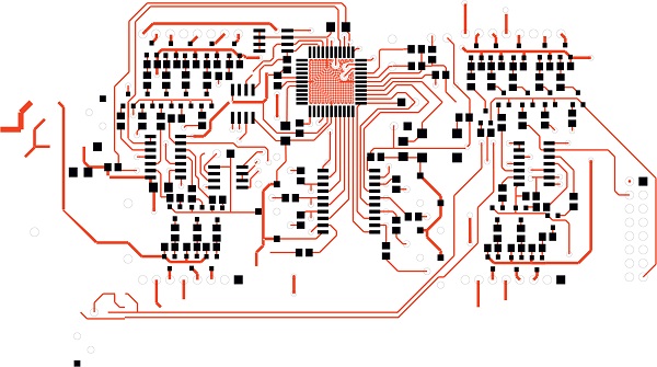
The process of building a good high speed PCB layout starts with the designing process. You have to be careful when drawing up the schematic and take many different possibilities into consideration. Add the details and maintain a smooth flow of the signal throughout the circuit. You want to highlight already in the schematics phase the critical and high speed signals and attached attributes such as trace lengths, add the value ranges, plot the terminations, show the impedance lines, and identify any potential areas that may produce noise. Some tools will show those attributes along the design phase and help support the layout phase.
The Right Material
Once the schematic design is ready to go, you need to select the right material for your high speed PCB. Each material or substrate has a different dielectric constant which has an effect on the impedance of a given transmission line. A lower relative dielectric constant means faster signal propagation in that material. Another factor to consider is the loss tangent which has the capacity to affect high frequency signal propagation. FR-4 and GETEK are two of the most commonly used substrates or materials for high speed PCB layouts.
PCB Stackup
When building a PCB, you will not get a guideline that states exactly how many layers you can add to it. Ideally though, you may be using a four layer PCB. it should have two signal layers accompanied by a GND and a VCC plane. This is in case of microstrip traces. If stripline traces are being used for a more complex circuit, then a six layer stackup is also recommended to reduce propagation delay and characteristic impedance. In a high speed PCB setup, you need to have at least one reference ground plane for the microstrip traces with sensitive signals. You should contact your PCB manufacturer to get some guidelines for more than 8 layers stackup.
Power and Ground Plane
Ideally, your high speed PCB should have a complete ground plane as well as a complete power plane. You should have a separate layer and ground plane for every regulated voltage you are using in your design. Instead of piling on the layers, some people choose to go with split ground planes. Unfortunately, these can produce radiations, create loop areas and block the flow of recurrent current, and give rise to crosstalk between signal lines.
- Two ground planes should not pass each other as they travel to the common ground. Keep their paths separate to reduce noise.
- Try your best to use complete ground and power planes. Do not split the plane.
- Instead of splitting, create functional blocks that do not influence or impact each other because they do not cross each other.
- If you have to use a split ground plane, minimize loop areas by avoiding routing over gaps.
- Make sure that the return current flows directly to the common ground.
- Split ground planes should only be connected at one point to reduce radiation.
- Power planes should not overlap with any ground plane other than their own.
- To reduce impedance at higher frequencies, make sure that the power plane is as close as possible to the ground plane to produce capacitive coupling between them.
Using Traces and Vias
Traces and vias are important components of a high speed PCB layout.
If you are using right angles in a trace, the capacitance in the corner of the angle increases which changes the impedance and produces reflections of current which can disrupt the signal transmission. Following are some methods you can use to prevent such disturbances:
- Instead of using right angle bends for your traces, cut the corner diagonally to produce two 45 degree corners.
- Ideally, a round bend is the best possible option to reduce reflections because of impedance changes.
- Try to keep high speed and low speed signals or digital and analog signals apart from each other with the help of strategic placement in the design and planning phase.
- Route signal layers perpendicular to each other to reduce crosstalk. We will further discuss crosstalk and ways to diminish it ahead.
- To prevent coupling, route the traces orthogonally to each other.
On the other hand, the use of vias can increase the trace length and it can also cause impedance changes because of added inductance and capacitance. Improper placement of vias can also create pockets of loop areas for current.
- Try not to use any vias in differential traces. If you have to use vias, then use them in both traces or compensate for the delay in the other trace.
- If your traces have sensitive signals, avoid using vias.
- To compensate for the problem of loop areas, you can add ground vias around the signal via to allow the return current to flow out beneath the signal trace.
- Do not place vias too close to each other as it can create lots in the ground place and make loop areas for return current.
Maintaining Signal Integrity
When traces are located right next to each other, they can unnecessarily and automatically be coupled in induction and capacitance. This sort of noise between parallel traces can interfere with other operations in the circuit which is why they need to be diminished or eliminated to maintain the integrity of the signal.
The key to reducing crosstalk between parallel traces is to increase the distance between them. Here are some techniques you can use to accomplish this:
- Use proper routing to maintain the signal integrity and prevent disruption from noise such as crosstalk. You can capitalize on the various signal integrity tools available to run simulations and find a clean trace for your PCB.
- If you are using a dual stripline layout with two signal layers placed next to each other, a good idea would be to route the traces perpendicularly to increase the distance between the layers but bring the layer and the reference plane closer together.
- Make it a habit to not bring traces closer than three times the height of the dielectric.
- Keep the signal lines as far away from each other during design and execution as possible.
- To keep the signals decoupled from each other, keep the transmission line as close to the ground plane as possible when designing.
- Try to keep parallel running sections short and minimize their number.
Reducing Ground Bounce
Ground bounce is a board level phenomena. These are essentially higher transient currents that are produced in the outputs by the discharge of load capacitances of the devices. The high current change on the signal causes fluctuations in the voltage. This issue is a consequence of faster devices that have decreased output switching time. In FPGAs, there are a number of different factors that impact the level and intensity of ground bounce produced in the chip, including the load capacitance of the devices, the inductance of the socket, as well as the amount of switching outputs used. Since the origin of ground bounce is multifactorial, it is difficult to predict its magnitude in the given PCB and only a relative approximation of the impact of each parameter can be made.
Following are some methods that can be used to reduce the amount of ground bounce produced in your high speed PCB:
- If you have any additional I/O pins, configure them as output pins and then drive the output value low to turn it into a virtual ground.
- Alternatively, you can make a programmable ground next to switching pins.
- Another way is to separate the I/O pins with ground pins interspersed between them manually.
- Eliminate sockets and pull up resistors whenever possible or use pull down resistors instead.
- Try to use multi layer PCBs with separate ground planes.
- Add decoupling capacitors, ideally very close to the power and ground pins. To maximize the current flow, you need to reduce the inductance in the decoupling capacitors. This can be done by connecting the capacitor to the power and ground planes with vias.
- Reducing series inductance can help reduce ground bounce as it limits momentary voltage drops from the power plane to the pin. This can be done to make the traces connecting the power plane and pins wide and short.
- Minimize the lead inductance by using low ESR capacitors that have very small values.
- Avoid using daisy chain connections as it increases inductance by increasing the return current loop. Try to connect each ground pin to the plane individually.
Termination
Reflection of signals in the lines due to mismatched impedance is another issue that can occur with high speed PCBs. This causes a ringing at the load receiver and also reduces its dynamic range. To prevent this from happening, we need to reduce or eliminate the mismatch in the impedance, meaning the source and trace impedance must be equal.
The impedance mismatch can be eliminated by adopting certain best practices in your termination scheme. Here are some tips to follow depending on which type of termination scheme you are using on your PCB:
- If you are using a simple parallel scheme, try to place the termination resistor very close to the load and keep the stub length from the resistor to the pin and pads at a minimum. If you have designed your board as such that you have no choice but to have a long termination line, then consider using a fly-by termination scheme.
- If you are using a Thevenin voltage divider, keep the length of the stub as small as possible and consider a fly-by termination in case of a long termination line to the receiver.
- Use a fly-by termination in an active parallel scheme.
- For a series-RC parallel termination, you need to balance the DC signalling so that signals are off half the time and on the other half. A fly-by can also be used here.
- In series termination, you can reduce reflection by adding another series resistor to match the signal source to the line impedance.
Transmission Lines
PCB level transmission lines can also cause trouble at higher frequencies due to mismatched impedance.
This impedance depends on the width and thickness of the trace, the dielectric constant of the material used for the PCB, and the height between the reference plane and the trace. Between the two types of layouts- stripline and microstrip- a typical stripline layout PCB has a slower rate of change with trace height above GND. It also has a signal that is bound between two layers of FR-4 material, while a microstrip layout PCB has a single conductor in the open air. Since a stripline layout has a higher and more effective dielectric constant, the dielectric span needs to be greater here as compared to microstrip layout PCBs to achieve the same impedance.
Clock Distribution
When it comes to the click distribution, it is possible to create a number of signal reflections that disrupt the optimum functioning of the high speed PCB because of the branches and trace lengths. Differing trace lengths can produce delays which also impairs the functioning of the board.
- To minimize this delay or eliminate it, it is important to keep the trace length for every clock signal at the same length.
- To distribute the clock signals evenly to all connected devices, a clock driver can be used.
- When designing the layout, take the possible delay for each trace into consideration and derive plans to compensate for it.
- Reducing the number of branches in the layout and preparing proper terminations can also help reduce reflections.


