SPI vs I2C: What is the Difference?
27/02/2023, hardwarebee
SPI and I2C are the two widely used serial communication protocols. Each communication protocol consists of its syntax and rules for data transmission between devices. In this article we will discuss the difference between SPI vs I2C, but first we will describe each protocol in details.
SPI – Serial Peripheral Interface
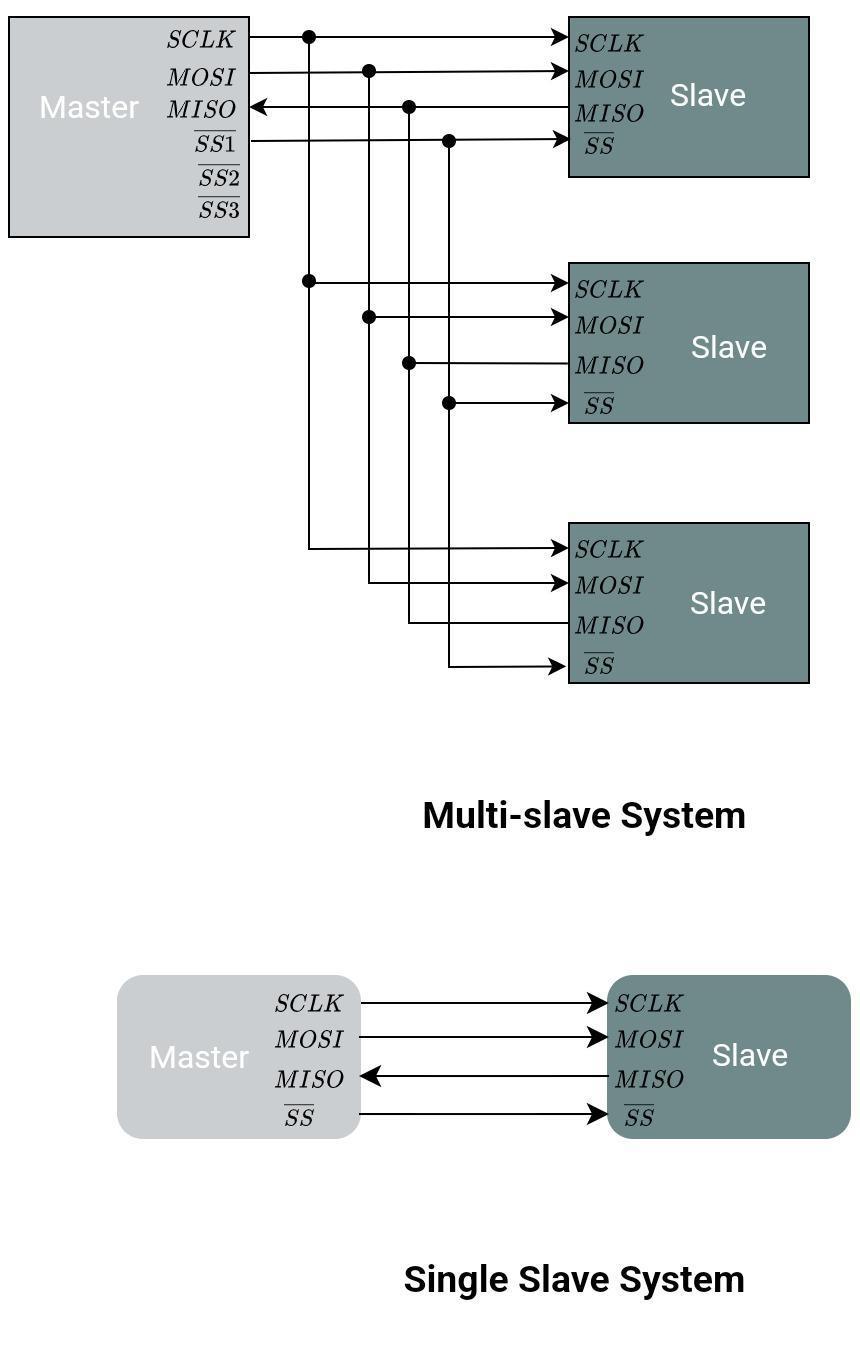
SPI is an acronym for Serial Peripheral Interface. Like I2C, it is also a serial communication protocol. It was developed by Motorola and allows sending and receiving data at the same time. It requires four wires to communicate between devices. These four wires include MOSI, MISO, SS, and SCLK. Since there is a line for the clock, SPI is a synchronous serial bus and is capable of working in full duplex and bidirectional mode. It means that the bus is capable of transmitting data in both directions at the same time. It supports a single-master and multi-slave system. Although it is slow, it is well-suited for onboard peripherals.
SPI Interface
SCLK (Clock):
In general, the clock signal is generated by the master and is used to synchronize data transfer between master and slave devices. Data is being transferred on the MOSI line. The slave then receives the clock pulses and data on the MOSI line.
MISO (Master In Slave Out):
The slave responds to the master using this MISO line. It responds by sending data on the same line. It transfers the requested data and information via this line.
SS/CS (Slave Select or Chip Select):
This pin remains low throughout the data transfer. It is useful when there are multiple slaves. It is an active low pin and is used to select the slave device. In I2C, there is a unique address for each slave device, but in SPI, there is a dedicated pin for selecting a specific slave. It is for initiating and terminating the data transfer to the particular slave.
Different Modes of SPI and Timing Diagram
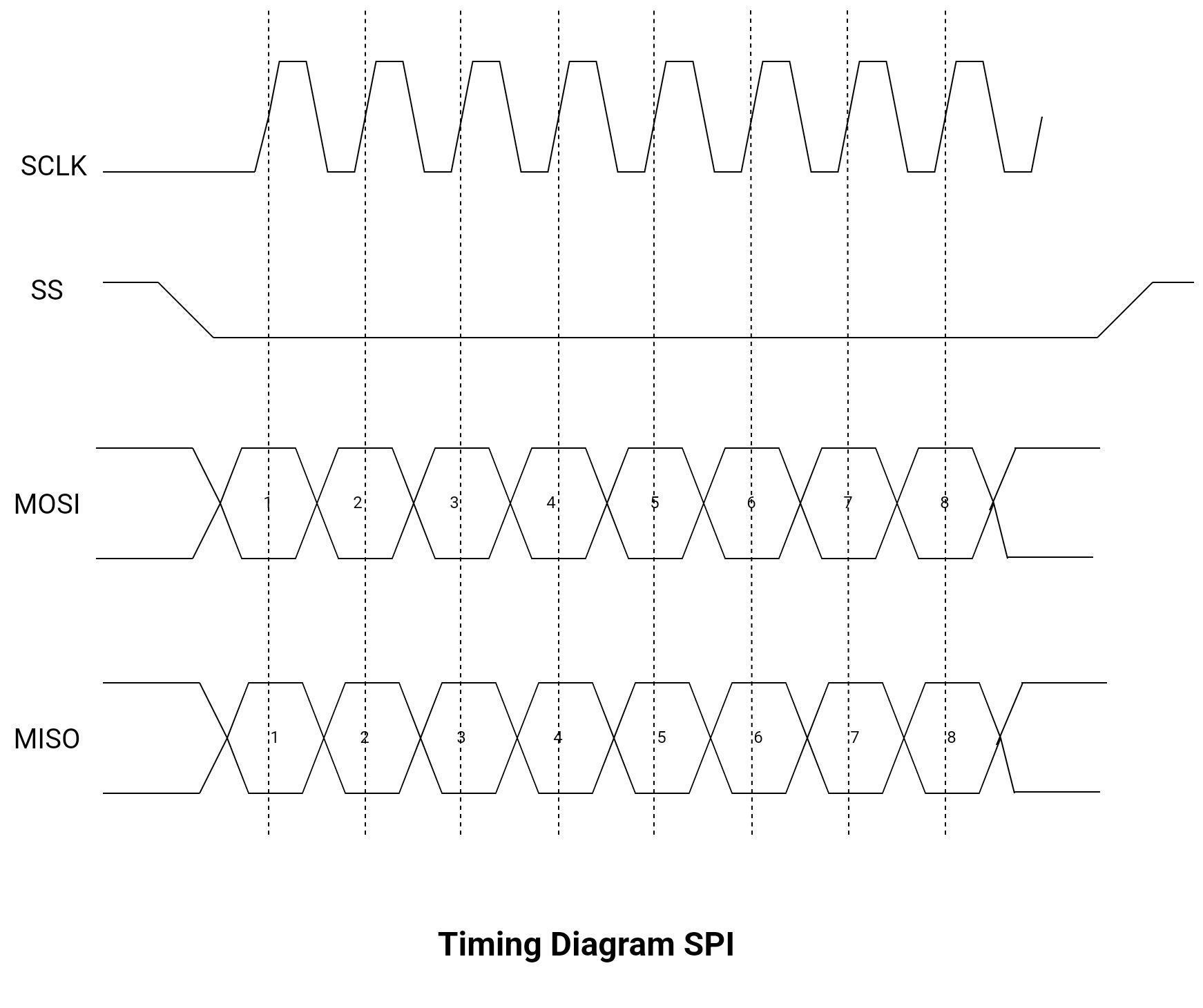
The timing diagram shows the relationship between clock signal SCLK, data input, and data output signals in an SPI communication. It has an 8- or 16-bit frame consisting of data only. There is no start bit, stop bit, parity bit, or ACK or NACK bit.
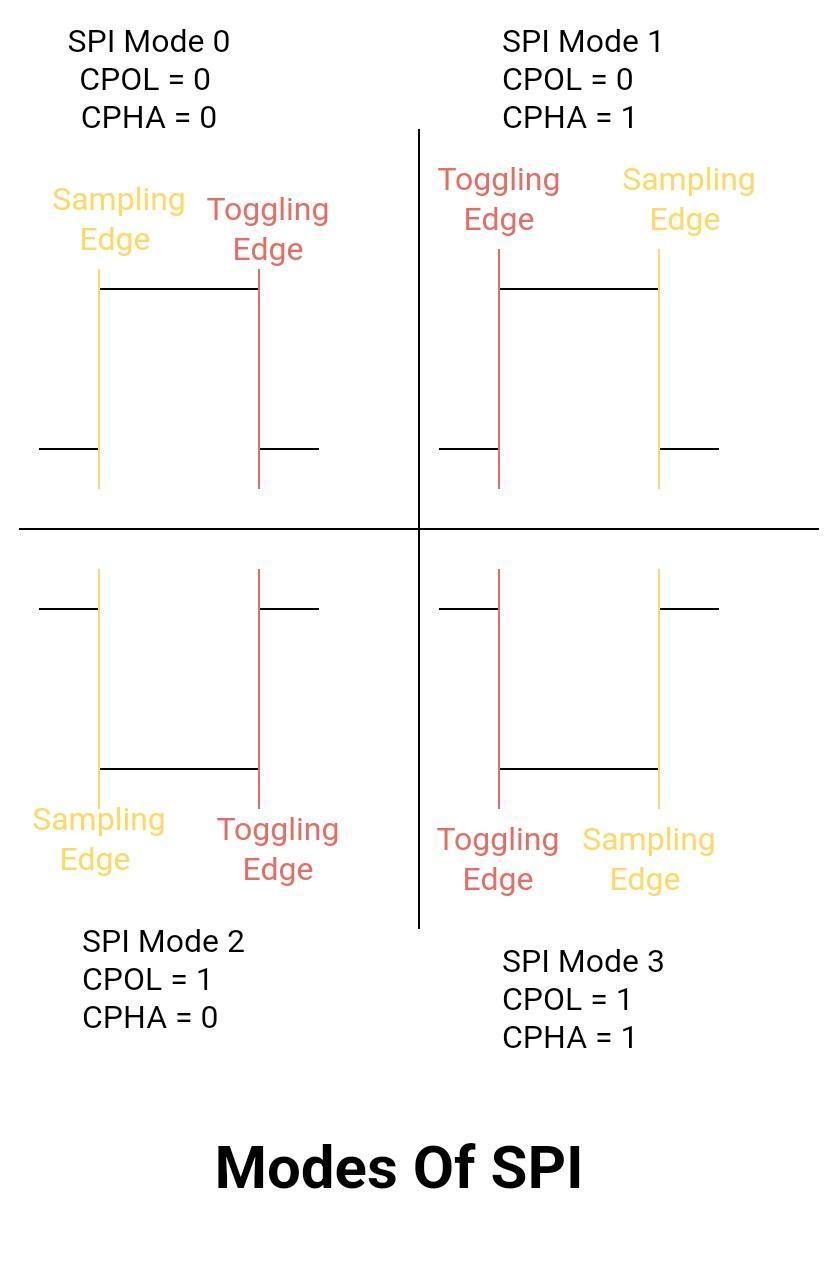
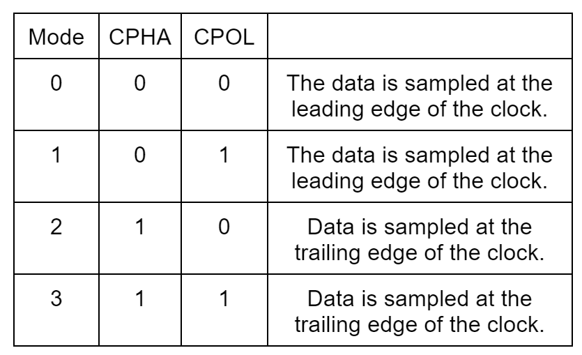
The timing diagram can largely depend on the SPI bus’s specific configuration, such as the clock phase and polarity and the number of data bits being transferred. There are four possible modes of operation based on clock phase and polarity. The master is responsible for configuring the clock frequency along with the clock polarity (CPOL) and clock phase (CPHA). The following diagram shows the possible states of these parameters.
CPHA:
CPHA determines which edges of the clock signal are used to drive and sample data signals. To put it another way, when the data must be sampled or toggled.
CPHA = 0: data is sampled at the leading edge of the clock.
CPHA = 1: Data is sampled at the trailing edge of the clock.
CPOL:
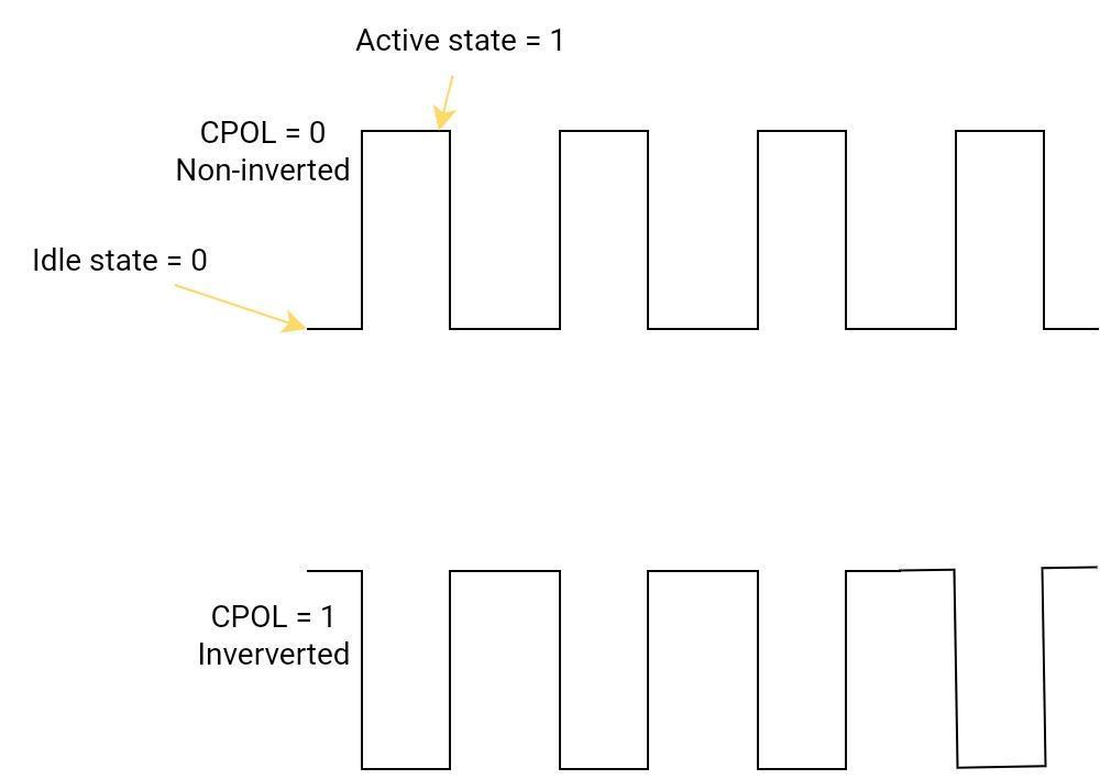
CPOL = 0: For non-inverted clock cycles In other words, the clock’s idle state is 0, and the active state is 1.
CPOL = 1: For inverted clock cycles
Working Principle
- To begin communication, the master generates the clock signal. The bus master configures the clock first, which is supported by the slave device.
- Data transfer between master and slave occurs in serial mode through MISO and MOSI lines.
- Select the slave and the SS line of that slave goes low.
- The master starts sending data bit by bit, starting with the MSB (the most significant bit) through the MOSI pin.
- The slave reads on the MOSI line.
- The slave sends a bit on the MISO line, and the master reads it on the MISO line.
- At the end of transmission, the SS pin goes back to high.
I2C – Inter Integrated Circuit
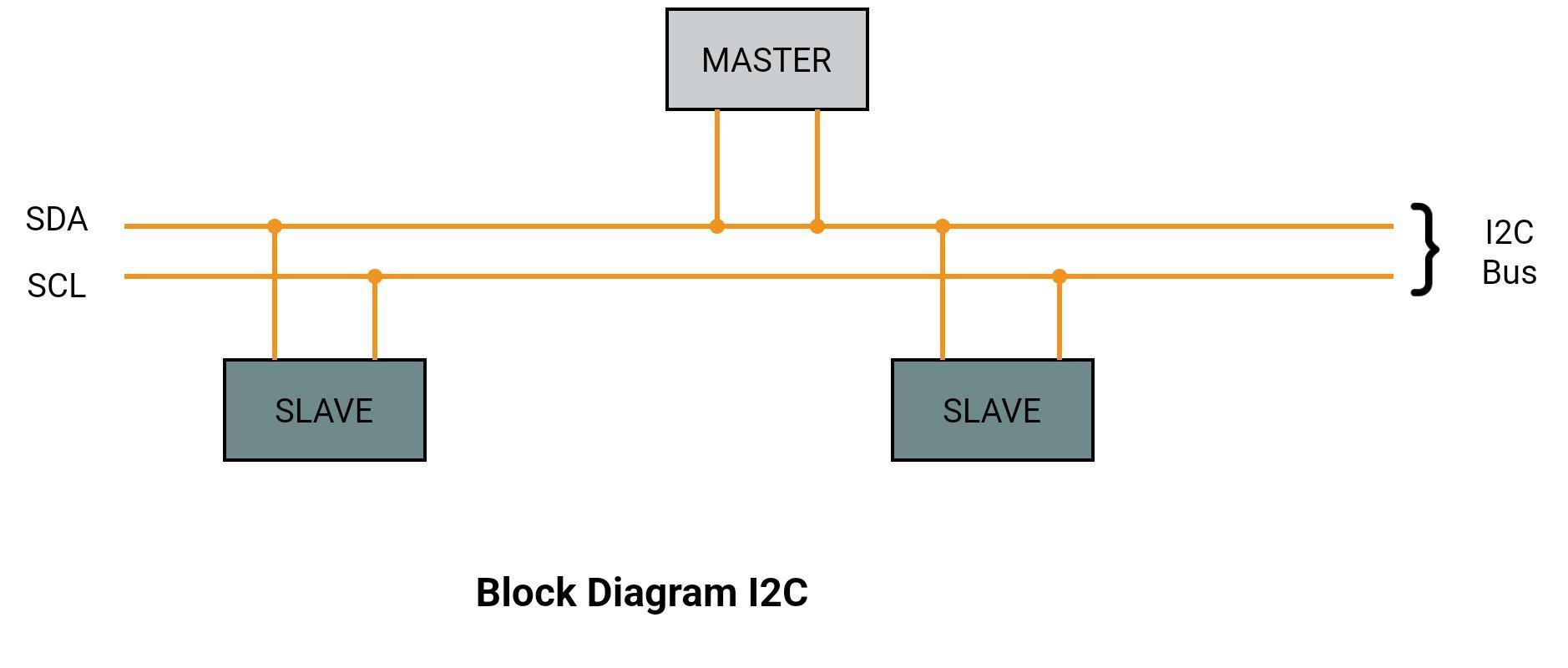
I2C is also known as I2C, IIC, and Inter IC. It is an acronym for Inter-Integrated circuits. Like SPI, it is also a serial communication protocol. It is developed by Philips Semiconductors. It is a half-duplex communication protocol. It can either receive or transmit information one at a time. It is well known for two-wire communication. The wires are labeled SCL (Serial Clock) and SDA (Serial Data). Since there is a clock, it is also synchronous communication. It is a master-to-slave communication protocol. It supports multi-master and multi-slave systems. All the information transfer between devices requires only two lines. This is possible because every device (slave) has a unique address.
It allows interconnecting multiple devices over a short distance using a common bus. Although it is slow, it is well-suited to inter-chip and intra-chip data transfer. All the devices attached to the network share the same bus for exchanging information. The protocol is beneficial, as is evident from the fact that it requires only two wires. A single bus can support up to 127 devices.
I2C Interface
To communicate data between devices, the I2C bus has only two signal lines. Both lines are bidirectional. There is no slave select or chip select signal. Instead of an SS signal, each slave has a particular address.
- SCL (Serial Clock)
- SDA (Serial Data)
SCL:
It carries a clock signal. In this protocol, data only transfers when this line is low. It means all the devices connected to this bus are active low. This is a master-slave protocol, and the SCL signal is controlled by the master device. All the data transfers are synchronized with the clock signal.
SDA:
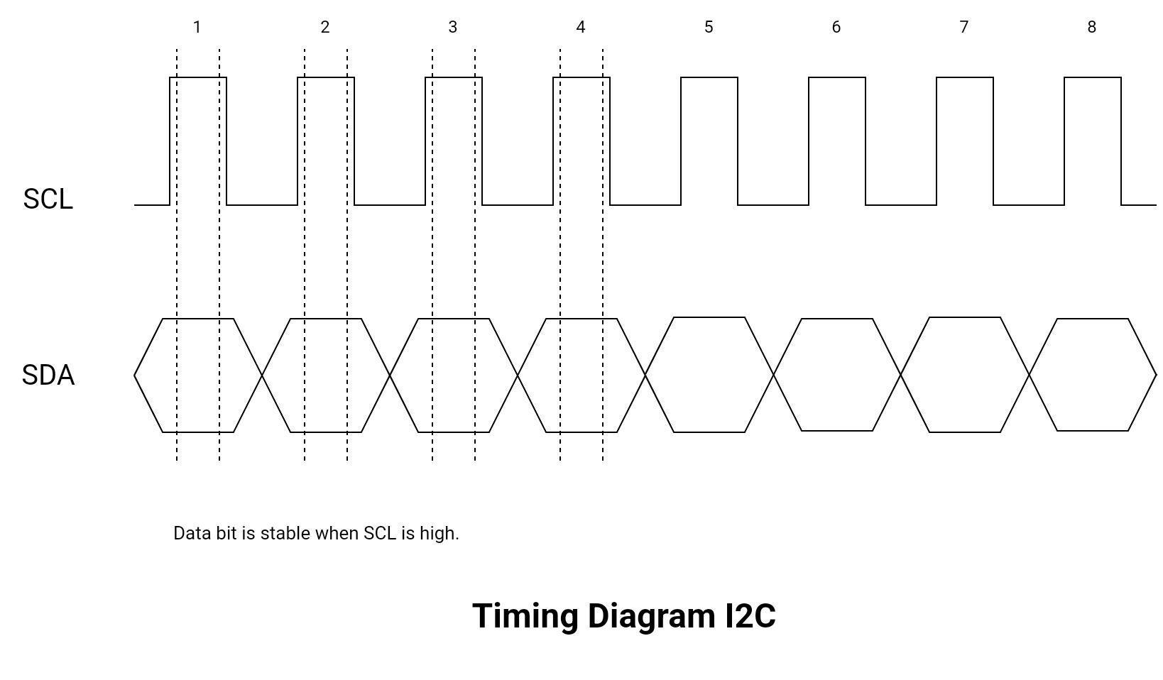
This line is dedicated to data transfer. A bus master is a device that initiates a data transfer on the bus while all other devices are considered bus slaves. The data on the SDA line can change if and only if SCL is logic low. Conversely, the data line is considered stable when SCL is logic high.
Timing Diagram And Data Transmission Protocol:
The I2C data transfer signal consists of the following components:
- Start (S)
- Stop (P)
- Repeated start (R)
- Data direction bit (Read/write bit)
- Address transmission
- Data
- Acknowledge (A)
Start Condition:
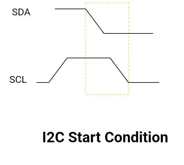
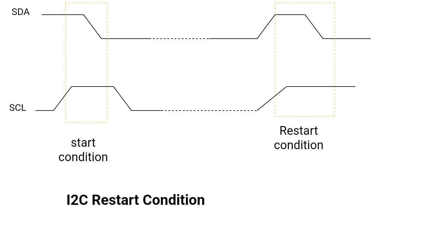
The START bit in the timing diagram is like an indication. It means that a device on a bus would like to communicate or transfer data on the bus. A start condition is recognized when the SDA line switches from high to low first, then the SCL line switches from high to low. In other words, a start condition occurs when the SDA line transitions from high to low, when SCL is high.
Stop Condition:
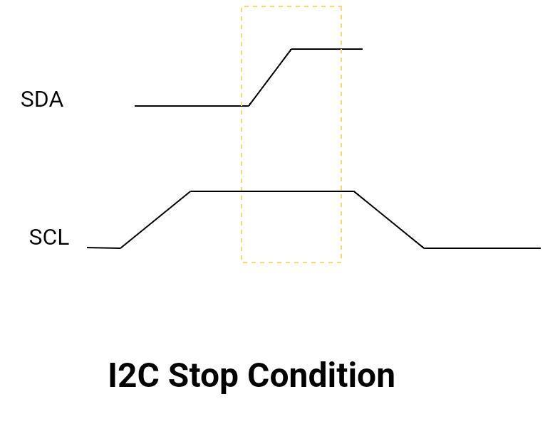
It is similar to the start condition. This occurs at the end of the data transfer. Once the data has transferred completely, this signal is generated by transitioning the SDA line from low to high when SCL is high. In other words, the SCL line goes high first, and then the SDA line transitions from low to high.
Repeated Start:
A repeated start occurs when the master device wishes to continue to transfer the data. Instead of sending a STOP condition and then resending a new START condition, it uses the Repeated START condition. In this condition, the master doesn’t release the bus and START a new communication with the same slave or with the other slave in different modes. The Repeated START condition illustrates in the timing diagram below.
Address Transmission:
As discussed earlier, the I2C protocol supports multiple slaves. After the start condition occurs, it is followed by the address of the particular slave. At the end of transmission, there is an ACK bit.
Data Direction Bit (Read Write bit):
This bit ensures whether the master wants to write to the slave or read from the slave.
- R/W = 0, to select the write operation.
- R/W = 0, to select the read operation.
Data:
After receiving read or write instructions (from the data direction bit), the data starts to transfer through the bus
The data is transmitted over the SDA line. The data is permitted to change only when the SCL line is low. Data is considered stable when the clock signal is high. Information is transferred in 8-bit packets along with an acknowledgment bit at the end. So, there are 9 SCL pulses required to transmit 8 bits of data and an ACK signal.
Acknowledge (A):
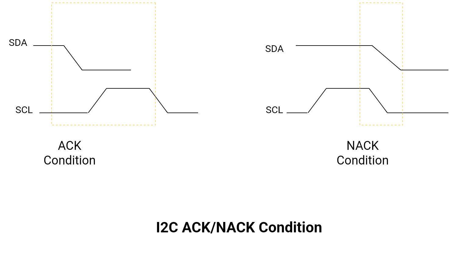
The device pulls the SDA line low to indicate that data transmission is successful, which results in an ACK bit. When an attempt fails, a NACK bit is returned to the sender. This acknowledgment occurs is at the end of every byte of data. When data is successfully received, the receiving device confirms it with the help of an ACK signal.
Working Principle
The I2C bus uses a controller (the master device) to control and communicate with slave devices. To send one byte of data, the following sequence is followed.
- A master always establishes the start condition for every slave connected on the bus.
- The address of the particular slave is sent over the bus.
- Every slave matches this address with its address.
- In the case of a matched address, the slave generates an ACK signal.
- The master sends the R/W bit to the slave.
- Master receives or transfers one byte of data.
- The receiving device generates ACK/NACK signals.
- To stop further transmission, the master sends a stop condition.
SPI VS I2C, What is the difference?
SPI and I2C are both commonly used serial communication protocols used for interfacing with electronic devices. While they share some similarities, they also have some significant differences.
SPI (Serial Peripheral Interface) and I2C (Inter-Integrated Circuit) are both synchronous communication protocols, which means that they require a clock signal to synchronize the communication between devices. However, the clock signal is handled differently in each protocol.
One major difference between SPI and I2C is the number of wires required for communication. SPI typically uses four wires: one for data (MOSI), one for data output (MISO), one for clock (SCK), and one for chip select (SS) to select the specific device being addressed. In contrast, I2C only uses two wires: one for data (SDA) and one for clock (SCL).
Another difference between SPI and I2C is their addressing schemes. In SPI, each device has a dedicated chip select (SS) line, which allows multiple devices to share the same bus. Each device is selected by pulling its corresponding chip select line low. In I2C, each device on the bus is assigned a unique address, which is used to select the device for communication.
Data transfer speed is another difference between SPI and I2C. SPI can typically achieve higher data transfer rates compared to I2C because it operates in full duplex mode (data can be transmitted in both directions simultaneously). I2C, on the other hand, operates in half-duplex mode (data can only be transmitted in one direction at a time).
Finally, the implementation of SPI and I2C can vary between different devices and manufacturers. It’s important to refer to the datasheet or reference manual of the device you’re working with to ensure you’re following the correct protocol.
In summary, SPI and I2C are both widely used serial communication protocols with their own unique advantages and disadvantages. SPI typically requires more wires and has a faster transfer rate, while I2C uses fewer wires and has a more flexible addressing scheme. The choice between SPI and I2C depends on the specific requirements of the application at hand.
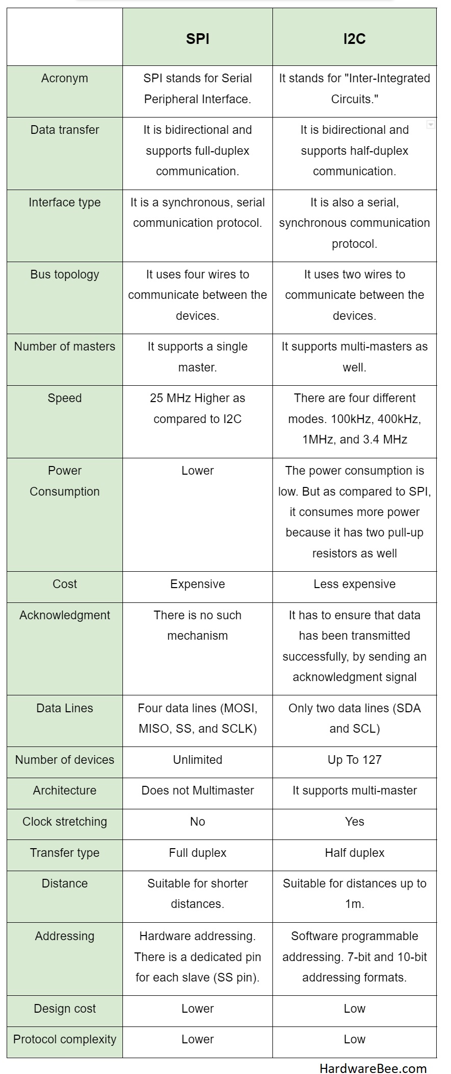
The table below shows the differece

