The Ultimate Guide to PCB Antennas
09/04/2024, hardwarebee
Introduction to PCB Antennas
In the communication industry, an antenna is a critical component, to allow transmit or receive electromagnetic waves. In the early age of antenna technology, the antenna was typically large, mounted on the external structure of the transmitter or receiver. The idea of a PCB antenna appeared in the early 1970s when antenna researchers started to investigate the use of a printed circuit board (PCB) instead of a separate antenna substrate. They intended to integrate antenna parts directly on the PCB, eliminating the need for separate substrates. Currently, the PCB antenna is a popular and promising alternative for wireless communication systems and electronics products.
Definition PCB Antennas
As the name indicates, the PCB antenna (Printed Circuit Board antenna) is an antenna whose physical structure is directly incorporated into the PCB. The antenna uses the PCB as a substrate, which is essential for physical size reduction. As a result, PCB antennas are increasingly being employed in situations where space is a significant concern.
Importance and Applications of Antennas on PCBs
In modern electronic devices with limited space, PCB antennas have brought multiple benefits due to their integration as a PCB component. The common importance and application of PCB antennas are discussed in this article.
Importance of Antennas on PCBs
PCB antennas are undeniably important in the electronics world, especially when device size is limited. First and foremost, PCB antennas enable compact integration that saves significant space. On the other hand, eliminating the external substrate decreases the cost of the PCB antenna. Moreover, the PCB antenna provides signal integrity by carefully positioning them on the board. On top of that, a PCB antenna provides some level of design freedom and allows integration with various device geometries.
Application of PCB Antenna
Due to its low profile, the PCB antenna may be used in many wireless applications. PCB antennas are widely used in communication systems and the Internet of Things (IoT) to establish a wireless link and data exchange. PCB antennas are also used in medical equipment and wearable gadgets for remote monitoring. Furthermore, in the automotive industry, PCB antennas are also utilized for Vehicle-to-Vehicle (V2V) or Vehicle-to Infrastructure (V2I) communication. Nowadays, a variety of consumer goods like smart TVs, gaming consoles, and home automation systems, employ PCB antennas for wireless access control.
Types of PCB Antennas
Although there are several PCB antenna types in antenna technology, some, such as horn, reflector, and waveguide antennas are difficult to integrate into PCB. This paper will briefly discuss the common PCB-embedded antenna types, which are:
- Microstrip Patch antenna: It is a planner antenna consisting of a radiating patch on the top and a ground plane at the bottom of the PCB. They may use contacting or coupling feeding techniques.
- Inverted –F antenna: The antenna’s radiating element is shaped like “F” and traced on the PCB. Feeding points are more commonly seen at the element’s junction.
- Printed monopole: A single radiating element printed on the PCB. This type of antenna is simple to design and emits omnidirectional radiation.
- Printed Dipole antenna: It consists of two radiating elements separated by a small gap. The radiating elements are oriented in a line and printed on PCB.
- Printed Loop antenna: a loop-shaped radiator printed on PCB either in a single or multiple turns. They are commonly used in magnetic field sensors.
- Slot antenna: An antenna printed on the PCB might contain one or more slots to improve radiation characteristics. Slot antennas are commonly used in RFID, radar systems, and other applications.
- Flexible antennas: Thin copper radiators are printed on fabric substrate for better flexibility. Most of these antennas are common in wearable applications and curved electronics.
Comparative Analysis
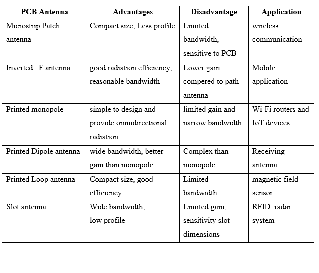
Table 1 illustrates a detailed comparative analysis of PCB antenna types, including their advantages, limitations, and most prevalent application areas.
Table 1 Comprehensive comparison of PCB antennas types and structure
Fundamentals of Antenna Design for PCBs
PCB antennas are designed on printed circuit boards, therefor designers must consider extra factors in addition to the fundamental antenna design principles. This paper introduces the basic concepts of general antenna design before moving on specialized issues for PCB antenna design.
Basic Principles of Antenna Design
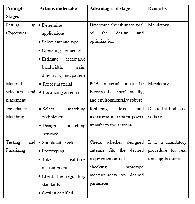
Antenna Engineers and researchers developed numerous concepts for antenna design. Table 2 summarizes the main principles across four stages of design in terms of actions undertaken, advantages, and other remarks in the design process.
Table 2 Summary of PCB antenna design principles
Key Parameters to Consider in PCB Antenna Design
In addition to the fundamental antenna design concepts mentioned above, PCB antenna designers must consider how the selection of PCB material, size, and shape impacts the electrical performance and mechanical strength of the PCB systems. The dielectric constant, loss tangent of material, thickness, and shape of the dielectric PCB material affects the performance of the PCB antenna. On the other hand, the proximity of the PCB antenna to other components also affects the performance. It requires excellent PCB layout design and antenna placement which minimizes interference due to electromagnetic coupling and enhances antenna performance. PCB antenna designers must be aware of the spacing, trace width, and compatibility of the antenna and must pass the PCB fabrication criteria.
Factors Influencing Antenna Performance on PCBs
Several factors affect the performance of PCB antennas. Understanding these factors is valuable in designing PCB antennas to enhance performance and reduce the degrading factors.
- Antenna Placement and PCB Layout: The proximity with other PCB components is determined by the location of the antenna on the PCB layout. Since it has a direct relation with antenna performance, careful placement of the antenna in PCB is demanded to minimize interferences and maximize the performance of the antenna.
- PCB Layout considerations for optimal design are the antenna must be far away from other PCB components, use a continuous ground plane, and trace the antenna to remove parasitic capacitance and inductances in the PCB.
- Frequency of Operation: It determines the dimensions of the antenna with respect to the wavelength. Small antennas in general less efficient, however, they are good at PCB integration. The larger the antennas have a good performance but it is not fit for small size integration.
- PCB Material: The loss tangent (tan δ), dielectric constant (εr) and thickness of PCB highly affect the performance of PCB antenna, proper design of feed line and matching network enhance PCB antenna performance with continuous ground plane. The selection of PCB material highly affects the radiation efficiency and bandwidth of the PCB antenna. The higher loss tangent increases loss and leads to the antenna being inefficient. A higher dielectric constant shrinks the physical size of the PCB with the cost of narrow bandwidth. The thicker PCB size is also good for bandwidth improvement with the cost of low radiation efficiency due to high loss in PCB in terms of surface wave.
- PCB fabrication and Packaging: The process also adds its own effect on the PCB antenna performance by introducing slight variations in antenna dimensions. The other factor that affects PCB antenna performances are environmental factors such as humidity, temperature, rain or obstruction, and building alter PCB antenna characteristics and must be taken into consideration during the designing process.
Techniques for Minimizing Interference and Maximizing Efficiency
In order to minimize the interference and maximize the efficiency of PCB antenna, the most typical strategies include utilizing antenna isolation, improving the impedance matching network, and applying a band-pass filter that rejects the unwanted propagations.
Implementation process of PCB Antenna
After the antenna is designed and finalized, the process of PCB antenna implementation is started. First, the PCB layout design is required to accommodate the antenna that must account to minimize interferences and maximize efficiency, and then trace all RF circuitry, impedance matching network, and antenna structure in accordance with the PCB layout. Second, develop a prototype for the designed PCB and test the performance of the antenna in terms of scattering parameter (S11), gain, radiation pattern, directivity, and other far-field radiation properties to ensure that the antenna achieves the desired objectives. If necessary, several iterations of optimization may be performed on the design until the desired performance is attained. Finally, arrange documentation for the manufacturer to assemble with the desired quantity and instructions for the user that offer explanations how to use the PCB integrated antenna.
Tips for Optimizing Antenna Performance on PCBs
This article provides the following advice for the optimization of PCB antenna to enhance its performance. As PCB material is used as a substrate of the antenna the designer must take strong care in the selection of PCB material. The material should with high-quality with low loss tangent and proper dielectric constant. Another strong recommendation is on the PCB layout design that is highly related to the surrounding interferences and enhancing the performance of the antenna. Additional care also considered impedance matching network, continuity of ground plane, minimizing obstructions from radiation patch, creating shielding, and use of filters for the antenna to reduce electromagnetic interferences. Lastly, if the designer is not an expert in RF and antenna technology, collaborate with experts to reassess the designed antenna and further optimization, especially in the testing and validation stage.
Common Pitfalls to Avoid During PCB Antenna Design
The most prevalent difficulties that PCB antenna designers face are while selecting PCB material. They undermine the effect of the PCB material and fail to recognize that it serves as a substrate for PCB antennas. They choose low-quality PCB material to minimize their initial cost of investing. This causes a substantial power loss of the PCB antenna in terms of heat, which possibly damages other PCB components and significantly reduces PCB antenna performance. Poor PCB layout is also a common mistake in PCB antenna design, it increases interferences and minimizes antenna efficiency. Some designers overlook the matching network, which results in major power reflection. Other typical pitfalls are insufficient ground plane for the PCB antenna, not considering environmental effects, distribution without careful simulation and testing of the antenna, and inadequate documentation for the manufacturer. Thus, PCB antenna designers and engineers must be aware of these pitfalls and try to avoid them as a proactive measure to enhance the quality of PCB antenna produces in terms of performance.
PCB Antenna Design Examples
This article provides examples of PCB antenna design specifically for NFC applications, Wi-Fi applications, Bluetooth, and RFID applications, along with a case study design overview and displaying corresponding selected performance metrics.
NFC PCB Antenna Design
Overview of NFC Integration on PCBs
NFC (Near-field communication) antennas are assisting the user for short-range wireless communication. They are designed to exchange information in a few centimeter ranges. These types of communication may be very important in contactless payment, secret data transfer, and access control.
Case study: NFC antenna design for contactless payment
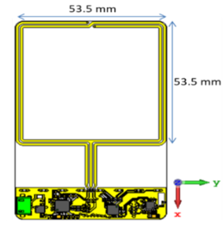
In the design of contactless payment, PCB integrated NFC antenna with an operating frequency of 13.5 MHz to communicate until the range of 10cm. The size of the PCB is approximated to the standard card size of 8.5 cm by 5.4 cm for the NFC reader. The rectangular loop antenna is selected and designed on 0.025mm thick FR4_epoxy PCB material with a 4.4 dielectric constant
Figure 1 Rectangular loop PCB antenna for NFC application
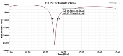
and loss tangent of 0.02. The design process including all matching networks as well as PCB layout is conducted on HFSS software as shown in Figure 1. The reflection coefficients of the designed PCB antenna are shown in Figure 2, which is dipped at 13.5 MHz with a bandwidth of 0.3 MHz
Figure 2 S11 plot of rectangular loop PCB antenna for NFC application
Challenges and Solutions for NFC antenna
There are many challenges in the case study design including the size of the antenna must be small and not more than the card size with acceptable antenna efficiency. On the other hand, the NFC antenna must be wideband to have a high data rate but as you see on the design the antenna has too narrow bandwidth. All efficiency, compact size, and wider bandwidth can be improved by iterative optimization through parametric analysis.
RFID Antenna Design
Overview of RFID
RFID is the acronym for Radio Frequency Identification, which is a wireless technology designed to track and identify items using an integrated PCB antenna. The application mainly uses LF, HF, and UHF frequency bands for wirelessly read or write data.
Case Study: RFID antenna for Inventory monitoring services
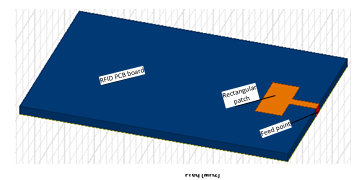
Now a day, smart warehouses are becoming popular and manage their properties by tagging RFID. The antenna is required to be small and efficient as well as operate in broad bandwidth. This case study will design a printed dipole antenna for inventory application in the UHF range of 860-960 MHz bandwidth. As shown in Figure 3, the patch antenna is designed on Roger material having 0.05 mm thickness, 2.2 dielectric constant, and 0.009 loss tangent.
Figure 3 Microstrip patch antenna integration on RFID card for inventory monitoring
Challenges and Solutions of RFID PCB antenna design
For inventory monitoring services, the RFID antenna has several challenges, mainly external electromagnetics interferences from Wi-Fi, Bluetooth, and cellular networks that affect the RFID signal. Physical obstruction and environmental factors also degrade the performance of the RFID antenna.
Wi-Fi Antenna Design
Introduction to Wi-Fi antenna design
Wireless Fidelity (Wi-Fi) allows to connect devices to the network over a distance range 10-100 meters. Wi-Fi is highly utilized for home, office or public hotspots. The operating frequency of Wi-Fi are 2.4 GHz as per IEEE 802.11b/g/n standard or 5 GHz per IEEE 802.11a/n/ac standard.
Examples of Designing Wi-Fi antenna for PCB layout
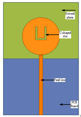
The printed U-slot antenna designed for Wi-Fi application is operated at a center frequency of 2.4 GHz (2.334 GHz -2.96 GHz), printed on the FR4-PCB with a size of 31mm x 33mm, loss tangent 0.02, and dielectric constant of 4.4, as shown in Figure 4. The antenna is designed and simulated using HFSS. The challenge of this design was the compactness of the antenna with the required performance.
Figure 4 U-slot printed PCB antenna for Wi-Fi application
Bluetooth antenna Design
Overview of Bluetooth antenna
Bluetooth is a short distance wireless technology to transfer data between connected devices in that range. It is commonly used in wireless speakers, printers, and headsets. The Bluetooth antenna is designed to operate at the ISM band of 2.4 GHz.
Designing a PCB integrated Bluetooth antenna
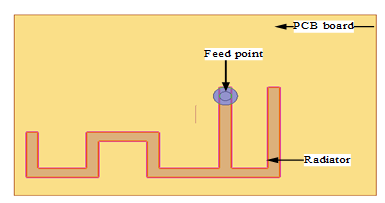
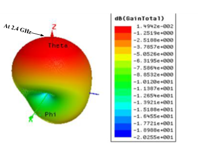
An Inverted-F antenna is selected for designing a PCB integrated Bluetooth antenna that operates at 2.4 GHz, as shown in Figure 5. The antenna is integrated into the PCB layout at the optimal location. The 3D gain pattern of designed antenna is presented in Figure 6.
Figure 5 Inverted-F printed antenna on PCB for Bluetooth applications
Figure 6 3D gain plot of the designed Bluetooth antenna
Factor affecting Bluetooth antenna performances
The Bluetooth antenna performance is affected by the antenna placement on the PCB, orientation of the antenna, internal, and external electromagnetic interferences. In addition, line of sight communication and distance from transmitter to receiver affect their performance.
Testing and Validation of PCB antenna
When the intended PCB antenna is nearing completion, the prototype must be tested and validated before real world deployment. The following measuring metrics are extremely significant in validating the prototype: Measure the S-parameter(S11), the gain, and the radiation pattern. If the PCB antenna has valued measured results and meets the simulation and the desired requirements, it can pass the validation unless re-designing or optimization is required.
Importance of Compliance Testing and Certification
It is strongly recommended and required that the finished products be tested and certified by regulatory authorities before the PCB antenna is commercialized. The PCB antenna appears to have been accepted by the legal regulatory body, and the testing result indicates that it is operating properly within the intended range of frequency at permissible radiation power.
Future Trends and Innovations in PCB antenna Technology
In the future, PCB antennas will be boosted by different emerging materials and antenna technologies. The upcoming metamaterial technology, fractal-shaped radiator as well as highly flexible fabric substrates are valuable for PCB antenna development. As the need for compact wireless electronics increases, so does the demand for PCB antennas. PCB antennas are predicted to become smaller, more efficient, and have a higher bandwidth in the future. They will be essential for next generation (B5G and 6G) wireless transmission in particular for mm-wave and terahertz communications.

