
Understanding Electronic Design Services Process
27/10/2018, hardwarebee
You might be interested in hiring an external electronic design services company to design your electronic product. Whether you have experience with an external electronic design services or not, this article will provide you with the necessary information to help you understand the electronic design services flow.
The process of electronic design consists of several steps that must work together to get best results. The steps consist of the following:
• Electronic Specifications
• Block Diagram
• Schematic Design
• PCB Layout
• Manufacturing
Each step must be followed and checked to ensure that the design is meeting product specifications and error free. It is true that some steps can be divided into 2 or more smaller steps, but the overall process of electronic product development follows these guidelines.
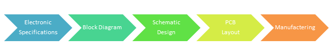
Figure 1: Electronic Design Services Steps
Electronic Specifications
This is a collection of product requirements and features such as: functionality, performance, cost, size, power consumption, operation modes, operating temperature, interfaces, standard compliance.
It’s a document that describes the product without getting into the implementation details. Its most likely that this is the most important phase in the entire electronic development phase because a mistake in this document will lead into designing the wrong product that will lead into months of delay (and extra cost). Therefore, you should take the necessary time to do the research and talk to customers, so you have the most accurate information.
The best approach is to base this document solely on customer interviews and inputs and not on your own interpretation of the market.
It’s expected that you create and deliver the electronic specifications to the electronic design company as it is your responsibility to specify the product.
Block Diagram
This is the first point where the electronic design company is taking the requirements and translating them into implementation. It’s a high-level design of the product in a block level with description of the interconnect of each block to other blocks or the external world.
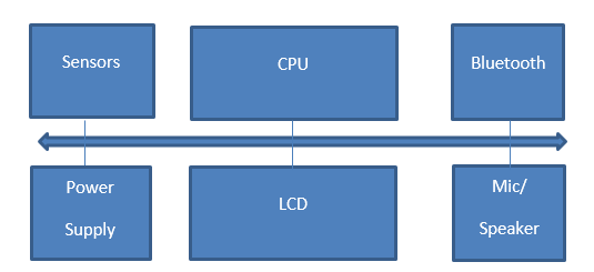
Figure 2: Block Diagram of a Smart Watch
It’s also a good time to choose the critical ICs for each block. Whether the product uses a micro-controller, FPGA or a WiFi chip – the electronic design company needs to identify these ICs and find out how they will connect to each other.
If possible, try to get the product cost. Once the major ICs are selected, one can use websites such as Avnet, Future or DigiKey to get a rough price estimate for each IC.
Schematic Design
Schematic design or schematic capture is the detailed electronic design of the electronic product. In this stage the electronic design services company is starting to use dedicated software tools to design the product.
In the schematic design stage, the design team is placing all ICs and passive components in a drawing sheet and thereafter, connecting all ICs pins and passive according to the product specifications. The wires represent the actual wiring between the different components.
In large design, there could be multiple design sheets with many ICs and other components.
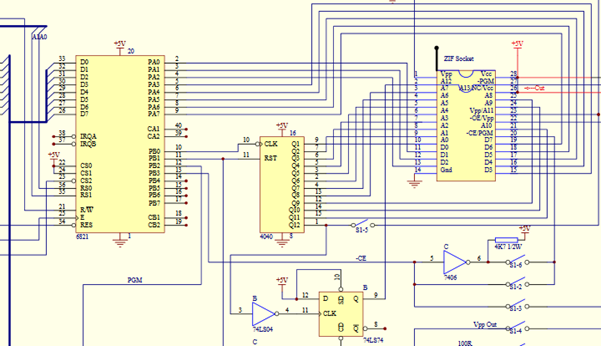
Figure 3: Schematics of an Electronic Product
At the end of this stage, the design services company can run simulation to verify the design, and provide accurate information about the product: size, cost, power consumption, bill of material, etc.
PCB Layout
Before going to production, the printed circuit board should be designed. This process is called layout and uses different electronic software tools. The layout process is a realization of the product on a target PCB (printed circuit board): placing all the ICs and the passives and routing all the wires between them according the schematic design.
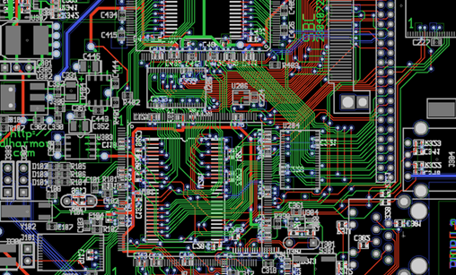
Figure 4: Layout example of an Electronic Product
In the PCB layout stage, the electronic design company needs to consider the product housing, location of connectors, power supply, etc.
The layout phase is the actual placement of ICs, passives and connections in real life. This is how the final PCB will be produced. At the end of this stage the electronic design services company will be able to deliver all the necessary files to produce the PCB (usually called gerber files).
If you are looking for an Electronic Design Services Company, please click here.


