The Ultimate Guide to Operational Amplifiers
11/07/2021, hardwarebee
In this guide, we presented the basic concepts of frequency domain analysis and how to apply it on electronic circuits. We also discussed filter topologies using resistors, capacitors, and inductors, which can be used to shape the frequency response of an input signal.
Now, we have enough background to analyze one of the most crucial components in electronic circuits: The Operational Amplifiers, also called Op-Amps. The Operational Amplifier is an active component composed by a large number of transistors, and its basic characteristic is voltage amplification. This device is very flexible, and can be applied to very different applications, such as signal amplification, active filtering, non-linear circuits, oscillators, and mathematical operations. The Operational Amplifiers receives this name because of its ability to perform mathematical operations, such as summation, subtraction, multiplication, etc. In this article, we will present the operational amplifiers in their ideal and real form, discussing the main characteristics and limitations of the device and provide real-life examples.
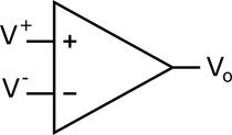
Figure 1: Operational Amplifier Symbol
The Ideal Operation Amplifiers
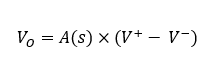
The operational amplifier is a three-terminal device capable of amplifying the voltage difference between two inputs V+ and V–, resulting in a voltage VO given by the equation ( is the amplifier’s open-loop gain):
![]()
Also, the ideal operational amplifier also has infinite input impedance, which means that the inputs act as open-circuits, with no current flowing into the amplifier. Finally, the ideal operational amplifier provides infinite open-loop gain (VO = infinity). Although this does not make sense in an open loop context, it is extremely useful in electronic analysis when feedback is applied. This is because, typically, the open loop gain of operational amplifiers is very large, allowing this simplification.
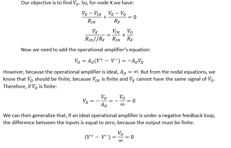
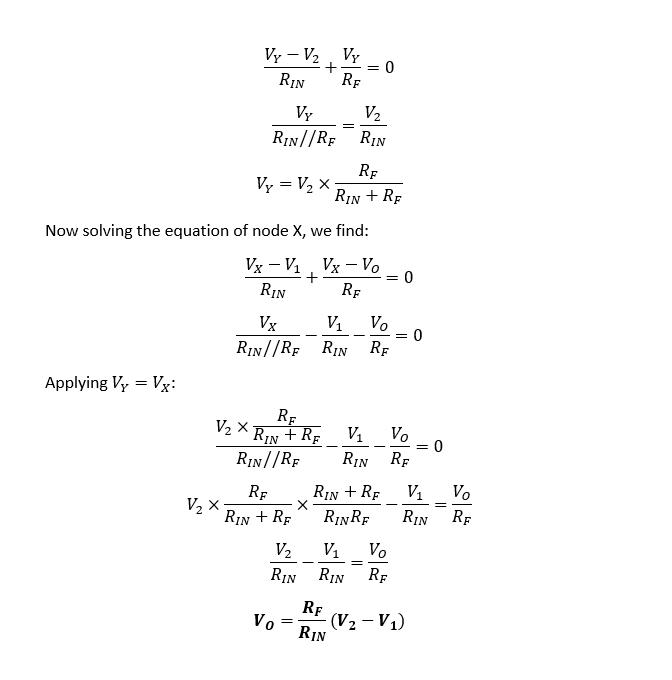
To understand how this can be applied, let us solve the nodal equations of the following circuit, where RF is providing negative feedback to the operational amplifier:
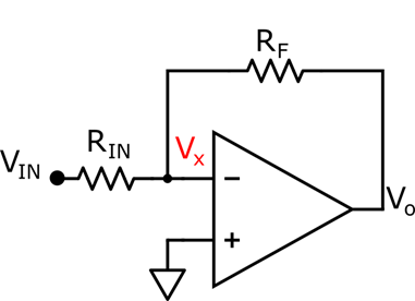
Figure 2: Circuit Example
Virtual Short-Circuit
Because ideal operational amplifiers, submitted to negative feedback, reduces the difference between the inputs to zero, the voltage of the inverting input V– is forced to be equal to the non-inverting input V+.
V– = V+
So, the inputs act as a short circuit. However, because there is no current flowing between the inputs, this “connection” is called a virtual short-circuit. This feature allows the control of one voltage by another voltage without direct connection and without current flow. In fact, the virtual short-circuit property is responsible for one of the most useful circuits in electronics: the voltage buffer.
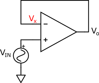
Figure 3: Voltage Buffer
If you need to copy the value of a voltage signal into a load but cannot afford to have current flowing from your signal source, the voltage buffer is the right circuit for the job. In this case, you can plug the signal source to the non-inverting input, which is copied to the inverting input via virtual short-circuit. The operational amplifier is then responsible for driving the necessary current.
Virtual Ground
The virtual ground is a consequence of the virtual short-circuit that can be used to simplify signal analysis. If the ideal operational amplifier is submitted to negative feedback, and the non-inverting input is connected to ground, one can simply consider , due to the virtual short-circuit. This is called virtual ground and can significantly reduce the amount of calculations during nodal solving.
The Inverting Amplifier
The main objective of an operational amplifier is to amplify signals. However, as we saw previously, it cannot use its infinite voltage gain to directly perform operations. Instead, a typical operational amplifier circuit applies negative feedback, and its infinite open-loop gain forces both inputs to be equal. Therefore, the voltage gain is not selected by the operational amplifier. Instead, it is the negative feedback that defines the overall gain of the amplifier circuit. We can exemplify this using the most basic amplifier topology: the inverting operational amplifier.
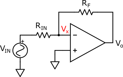
Figure 4: The Inverting Amplifier
Because of the negative feedback, we can apply the virtual ground concept at node X. Therefore, Vx=0V and the nodal equation is simply:
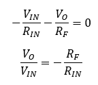
Therefore, the circuit provides an inverting gain proportional to the ratio between and . This gain is also called closed-loop gain. Therefore, the voltage gain can be easily changed by just replacing of varying the feedback resistors without modifying the operational amplifier. This example shows how flexible operational amplifiers can be.
The Non-Inverting Amplifier
Another famous amplifier topology is the non-inverting amplifier. In this case, the gain is positive, and proportional to the ratio between the operational amplifiers. To analyze this circuit, we can apply the virtual short-circuit concept, forcing VX to be equal to VIN. In this case, the nodal equations are simplified to:
Figure 5: The Non-Inverting Amplifier
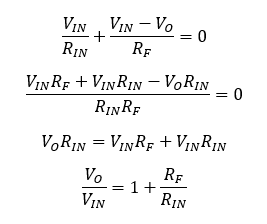
Notice that the gain is similar to the inverting one, with the addition of a “+ 1” term.
The Real Operational Amplifier
The ideal operational amplifier is a useful concept that can significantly simplify the solving process of amplifier circuits. However, real world operational amplifiers have finite open-loop gain, and this gain is also frequency dependent. Therefore, using the ideal operational amplifier model may introduce big calculation errors when applying amplifiers with low gain at the desired frequency.
Finite Open-Loop Gain
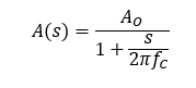
When dealing with amplifiers with small open-loop gain, one cannot apply the ideal operational amplifier model. Also, when the closed-loop gain is not at least ten times smaller than the open-loop gain, the calculation error may not be tolerable. In this cases, one can simply apply the basic operational amplifier equation: Vo=A0(V+ – V–). Considering that the gain is frequency dependent, we can use the Laplace transform to calculate the output voltage:
Compensated operational amplifiers present a first-order low-pass response. A first-order low-pass can be described by the low-pass filter equations presented in the Part II of this tutorial. In this case, the response is described by a DC gain A0 and a cut-off frequency Fc :
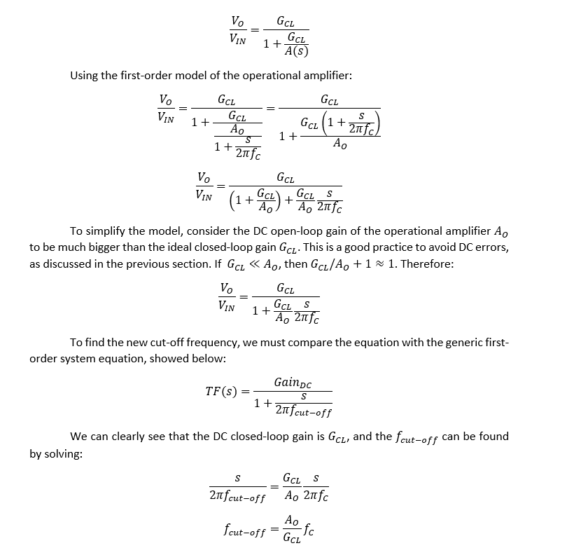
Notice that this response changes both magnitude and phase of the amplifier’s response. Let us apply this equation to the non-inverting amplifier circuit, instead of the virtual short-circuit assumption, to see how this affects the final result:
We start with the nodal equations. However, we should not consider Vx=Vin in this case, for node X:
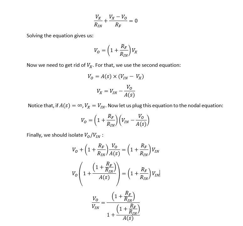
Now, this equation may seem a little frightening. However, let us simplify its meaning. Consider that the ideal closed-loop gain is called Gcl. Then:

Now we can clearly see that: if the open-loop gain A(s) tends to infinite, the transfer function becomes equal to Gcl and we can apply the ideal operational amplifier model. Also, if Gcl<<|A(s)|, the denominator is almost 1 and we also have the ideal operational amplifier case. However, as the modulus of A(s) decreases in frequency, or if we design a Gcl that is too big, the denominator increases and the transfer function deviates from the ideal case, reducing the real gain of the circuit.
These conclusions are valid for most amplifier configurations, not only the non-inverting case, although the actual transfer function can differ greatly from one to another. Therefore, comparing the open-loop gain to the desired closed-loop gain is important to select the operational amplifier model for analysis.
Frequency Dependent Gain
The previous approach is enough to solve most of circuits using operational amplifiers when negative feedback is applied. However, it is not very practical for fast analysis, especially when we consider the dependence of gain on frequency. To gain some intuition, let us analyze graphically how the open-loop gain changes the closed-loop gain in frequency.
Considering the first-order model of an operational amplifier, the bode plot of the open-loop gain can be seen below:
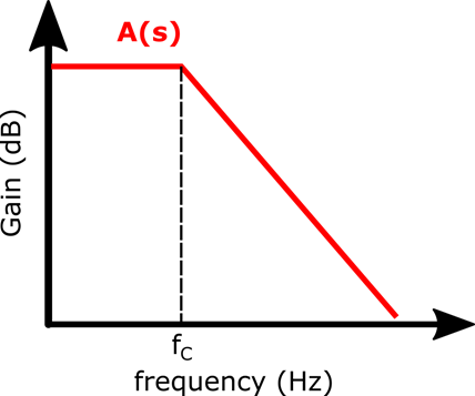
Figure 6: Open-Loop Gain of a First-Order Operational Amplifier
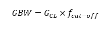
Now, using the non-inverting amplifier equation found before, we can find the closed-loop cut-off frequency of this amplifier (keep in mind that Gcl=1+Rf/Rin ):
Therefore, one can find the closed-loop bandwidth of a non-inverting amplifier by simply applying the previous equation. Also, we can see that the bigger the closed-loop gain, smaller the bandwidth. Because of the gain versus frequency trade-off, compensated operational amplifiers typically have a fixed gain-bandwidth product, called GBW, which is equal to:
So, to find the bandwidth for a given gain, one can simply divide the GBW by the closed-loop gain, and vice-versa. Finally, to get even more insight, let us find the value of the open-loop gain at the closed-loop cut-off frequency. To do so, we need to plug Fcut-off into the first order operational amplifier model:
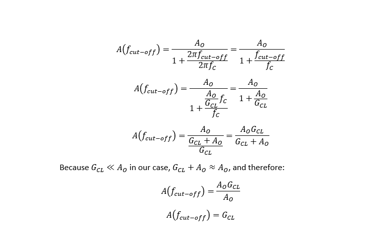
This result is very important in real operational amplifier analysis because it tells us that the cut-off frequency of the closed-loop gain occurs at the point where the open-loop gain is equal to the closed-loop gain. Figure 7 shows how this affects the gain graphically. Therefore, one can use the open-loop gain bode plot to predict the closed-loop frequency behavior of the amplifier.
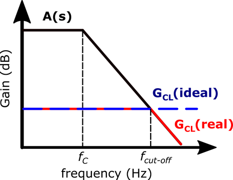
Figure 7: Bode Plot of the open-loop gain (black) and the ideal (blue) and real (red) closed-loop gain of a non-inverting amplifier
Operational Amplifiers Applications
Because of its flexibility, operational amplifiers are used in many applications. We already presented some basic topologies of amplifiers and the voltage buffer. Here, we will quickly analyze a differential amplifier and a voltage controlled current source.
Differential Amplifier
The objective of the differential amplifier is to perform the subtraction of two signals. This operation is extremely important in instrumentation, to reject the common mode voltage of small differential signals, that usually come from sensors. It is the heart of the instrumentation amplifier.
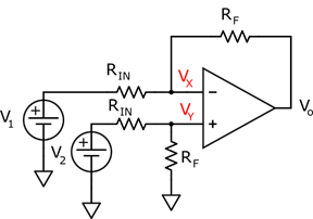
Figure 8: Differential Amplifier
To understand how the topology works, it is useful to apply the ideal model of the operational amplifier. The virtual short-circuit forces Vy=Vx . Using the nodal equation of node Y, we can find the voltage Vy:
This final result gives us the function that describes the differential amplifier: it applies a gain of Rf/Rin to the difference between both inputs.
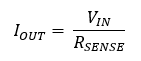
Voltage Controlled Current Source
Operational amplifiers can also be combined with a transistor to provide electric current that can be controlled linearly by a small input voltage, which is very useful to drive . The circuit is shown in the figure below.
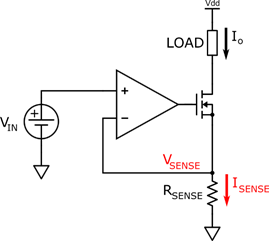
Figure 9: Voltage Controlled Current Source
Similar to the previous analysis, we can apply the ideal operational amplifier model. Using the virtual short-circuit, we can already see that the voltage Vsense must be equal to the input voltage:
Vsense=Vin
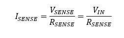
Therefore, the current passing through the resistor Rsesnse is simply defined by:
The MOSFET presents a gate current of zero, and therefore the drain current must be the same as the source current, which is Isesnse. Also, the MOSFET provides more current driving capabilities than the operational amplifier, and a high output impedance that is required of a current source. Therefore, the output current of the voltage controlled current source is simply: