
Understanding Clamper Circuit
19/12/2022, hardwarebee
Introduction
A clamper circuit is an electronic circuit using a resistor, capacitor, and diode to shift up or down a signal without changing the signal shape. In fact, this circuit adds a positive or negative DC offset to the signal. In some cases, a dc voltage source like a battery can be used together with the mentioned element to shift the signal. Thus, the clamper circuits can be categorized into positive, negative, and biased clamper circuits. These types of clamper circuits are discussed comprehensively in this article using equations, signals, and examples.
Positive Clamper Circuit
The first type is a positive clamper circuit that shifts up the input signals without changing the appearance of the signal. Therefore, any kind of input signal can be used in this circuit, including square-wave or sinusoidal. The positive clamper circuit is shown in Figure 1, having a sinusoidal voltage source, a capacitor, a diode, and a resistor. The output voltage would be the voltage across the load resistor.
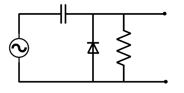
Figure 1: Positive clamper circuit
Before analyzing this circuit, it should be noted that the RC time constant in this circuit must be larger than the time period of the input signal. Practically, it is assumed that the time constant should be ten times greater than the period. The diode and capacitor behavior must be checked in positive and negative half cycles to analyze the circuit. At the first instant, the capacitor is discharged and acts as a short circuit. Therefore, the cathode voltage of the diode will be greater than the anode voltage, and the diode will be in reverse bias. In this mode, the ideal diode is open-circuited, and the capacitor is charged through the path to the resistive load, as shown in Figure 2. However, the RC time constant is considerably large, meaning that the capacitor needs more time to be charged. Thus, it can be assumed that the output voltage is equal to the input voltage.
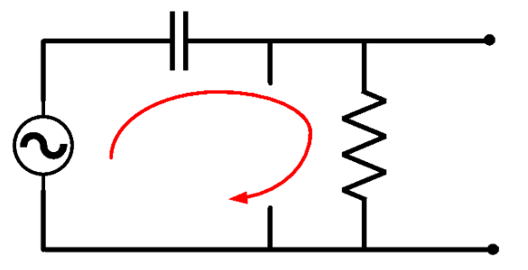
Figure 2: Positive clamper circuit in positive half cycle
In the negative half cycle, the situation is the opposite, and the diode is in forward bias. Hence, the diode is short-circuited, and the voltage across the load is zero. As indicated in Figure 3, the capacitor is charged to Vm. When the input voltage passes the negative peak voltage, the voltage across the diode (Vin+Vm) gets positive, showing that the diode is in reverse bias, and the current can flow through the load. In fact, when the input voltage is –Vm, the output voltage will be zero, while the output voltage is Vm when the input voltage is zero.
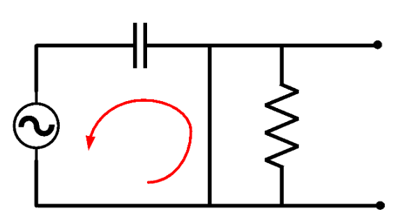
Figure 3: Positive clamper circuit in negative half cycle
It can be said that after the first negative peak voltage, the output voltage can be obtained by using the following equation.
Vout=Vin+Vm (1)
In the next positive half cycle, the situation is the same as the first positive half cycle, and the diode is open-circuited. Hence, the output voltage follows Equation (1), and in the peak voltage, the output voltage will reach 2Vm. Similarly, in a zero-crossing point, the output voltage will be equal to Vm. The next cycles follow the same procedure, and the steady state output voltage has a positive DC offset compared to the input voltage. The input and output signals are illustrated in Figure 4. In this figure, a transient state is available, which is related to the first cycle, and it is eliminated in the following cycles.
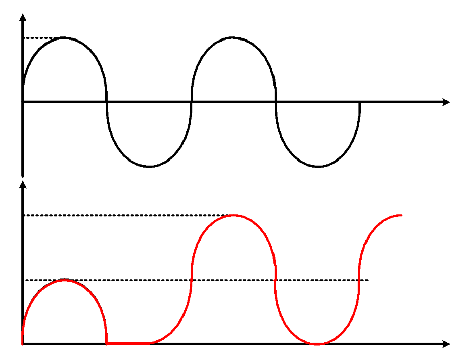
Figure 4: Input and output voltages in positive clamper circuit
The negative clamper circuit is presented in the next section, which follows the same principles as the positive clamper circuit.
Negative Clamper Circuit
The negative clamper circuit is built by just reversing the diode in the positive clamper circuit, as shown in Figure 5. As the theory behind this circuit is similar to the positive clamper circuit, a square-wave source is used for better understanding in this analysis. It is expected that the input voltage is sifted down to create the output voltage.
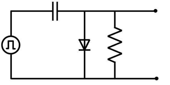
Figure 5: Negative clamper circuit
In the positive half cycle, the anode voltage is greater than the cathode voltage, and the diode is in forward bias. Therefore, the capacitor is charged in this case, and the output voltage is zero because the diode is short-circuited.
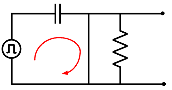
Figure 6: Negative clamper circuit in the first positive half cycle
In contrast, the diode is in reverse bias in negative half cycle, and the voltage across the load resistor is equal to –(Vin+Vm) because the diode is in reverse bias, as shown in Figure 7. Since the input voltage in negative half cycle in square-wave signal is –Vm, the output voltage would be -2Vm.
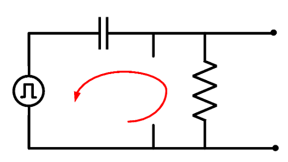
Figure 7: Negative clamper circuit in the first negative half cycle
In the next half cycle, the diode is again in forward bias because the capacitor voltage has been reduced in the previous half cycle. Thus, the output voltage will be zero in the second positive half cycle. Following this procedure, the output voltage will be like Figure 8 with a negative DC offset.
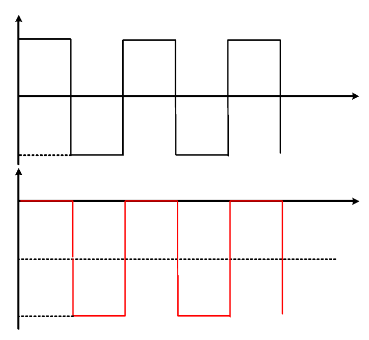
Figure 8: Input and output voltages in negative clamper circuit
Biased Clamper Circuit
This circuit is used to obtain additional voltage swings. To achieve this goal, a DC voltage source is added to a positive or negative clamper circuit to create a DC offset of less or more than Vm. The voltage DC source can be a battery, which is series with the diode in the parallel branch, as shown in Figure 9. It is assumed that Vin is greater than Vdc.
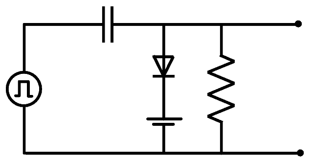
Figure 9: Negative clamper circuit with biasing voltage
In the positive half cycle, the diode is short-circuited, and the voltage across the load resistor is equal to Vdc. Moreover, the capacitor gets charged in this positive half cycle with the voltage of Vm–Vdc. In the negative half cycle, the diode turns off, and the output voltage will be -2Vm+Vdc. The procedure is the same in the following cycles, and the output voltage will be like the presented signal in Figure 10.
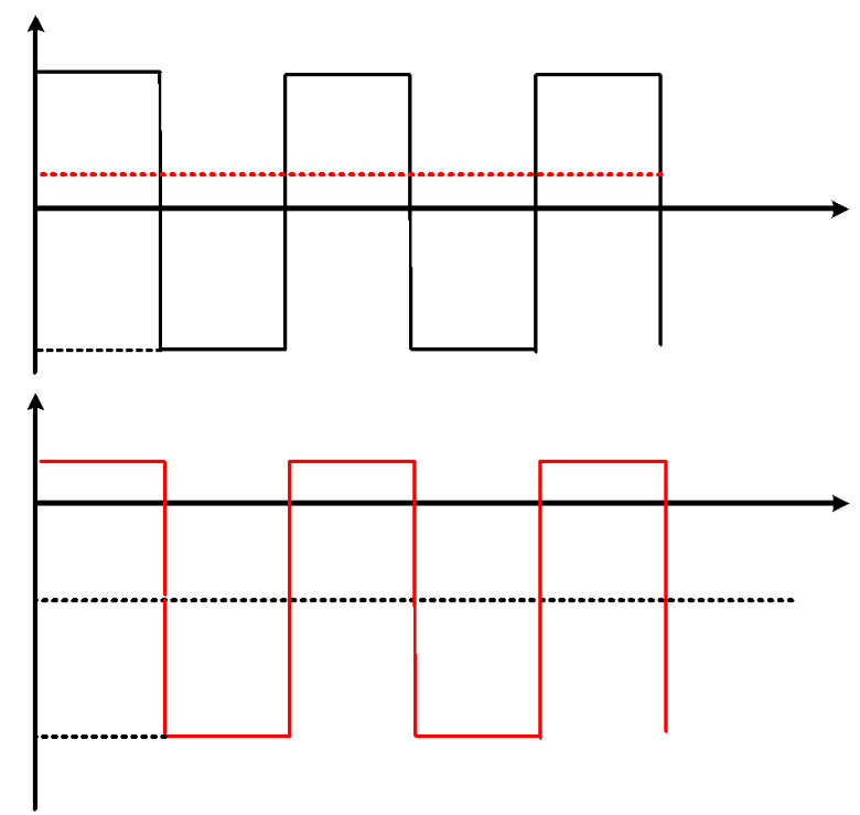
Figure 10: Input and output voltages for negative clamper circuit with biasing voltage
Clamper Circuit vs. Clipper Circuit
There are many differences between clamper and clipper circuits. In a clamper circuit, the goal is to shift the signal without changing its shape, while a clipper circuit removes a portion of the signal and changes its shape. In fact, a clipper circuit is used to limit the signal amplitude, but the clamper just moves the signal up and down. In a clipper circuit, there is no capacitor, and the diode is in series with the source, but the clamper circuit requires a capacitor, and the diode is in parallel with the voltage source.
For better understanding, an example circuit of a clipper circuit is presented in this section. As mentioned, the clipper circuit prevents the output signal from exceeding a certain level and changes its shape by chopping a part of the waveform. The simplest form of clipper circuit is a half-wave rectifier, which eliminates the positive or negative cycle of input voltage. Thus, energy-storage elements are not required for this circuit. Figure 11 depicts the clipper circuit with biasing voltage that chops the voltage while it is greater than the reference voltage (Vdc).
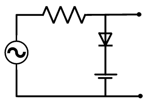
Figure 11: Clipper circuit with biasing voltage
As can be seen, a DC voltage source is in series with the diode to determine the reference voltage for protection purposes. When Vin is lower than Vdc, the diode is open-circuited, and the output voltage mimics the input voltage. However, once the input voltage exceeds the reference voltage, the diode acts as a short circuit. Therefore, the output voltage will be equal to the reference voltage. As a result, the output voltage cannot go higher than the reference voltage, as shown in Figure 12.
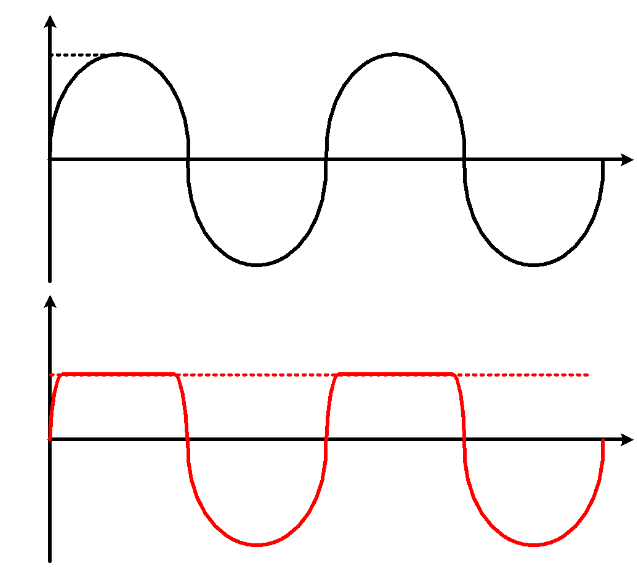
Figure 12: Output voltage of a biased clipper circuit
Clamper Circuit Applications
This circuit is widely used in various devices, such as television circuits and voltage multipliers. Moreover, amplifiers are protected against large errant signals using clamper circuits. Test equipment, sonar, and radar systems also have clamper circuits. Furthermore, distortions can be removed, and this circuit can enhance overdrive recovery time.
Clamper circuits are widely used in various electronic applications. Some common applications of clamper circuits are:
- DC restoration: Clamper circuits are used to restore the DC component of a signal that has been distorted or lost due to capacitive coupling or other factors.
- DC bias: Clamper circuits can be used to add a DC bias to an AC signal, which is useful in applications such as audio amplifiers and oscillators.
- Waveform shaping: Clamper circuits can be used to shape the waveform of an AC signal, which is useful in applications such as pulse width modulation (PWM) and pulse code modulation (PCM).
- Noise reduction: Clamper circuits can be used to reduce noise in electronic circuits by eliminating the AC component of a signal.
- Amplitude modulation: Clamper circuits can be used to modulate the amplitude of an AC signal, which is useful in applications such as radio transmission.
- Signal coupling: Clamper circuits can be used to couple two signals together, which is useful in applications such as signal processing and data transmission.
- Circuit protection: Clamper circuits can be used to protect electronic circuits from high voltage spikes or other damaging events.


