
Configurable Logic Block (CLB)
08/04/2021, hardwarebee
What is Configurable Logic Block (CLB)?
A configurable logic block (CLB) is the basic repeating logic block on an FPGA. There are hundreds of similar logic block available onto the FPGA connected via routing resources. The purpose of these logic blocks is to implement combinational and sequential logic.
There are three essential CLBs components:
- Flip-Flops
- Look-up Tables (LUTs)
- Multiplexers
Flip-Flop — Flip-Flop is a single bit storage element available onto the FPGA.
Look-up Table (LUT) — A LUT is the heart of the FPGA. It contains all the logically possible output of your design. LUT are mux-based architecture in which the inputs are the possible outputs based on the correct selection on the multiplexer select lines.
Multiplexer—A circuit does the transitions between different outputs based on the select lines inputs.
Xilinx FPGA is mainly composed of the following unit structures: configurable logic block (CLB), clock management module (CMT), memory (RAM/FIFO), digital signal processing module (DSP) and some unique modules.
CLB is the leading resource containing the design logic in FPGA and the main functionality in logic design. CLBs realize the logic of FPGA configured in an array. Each CLB part is connected to a switch array and controlled by it to implement the logic, as shown in Figure 3.
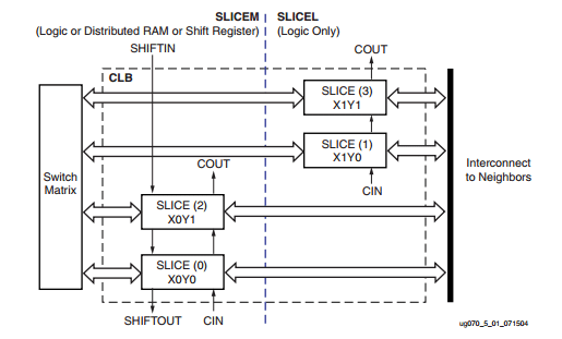
Figure 3: Xilinx CLB
Each CLB contains two basic structures called Slice; each basic Slice contains 4 look-up tables, 4 storage units, a wide function multiplexer, and carry logic; this basic structure (Slice) is called SLICEL. Besides, some Slice also includes using RAM to store data and the function of shifting using 32-bit registers. The basic structure that supports these functions is called SLICEM.
The clock management module (CMM) is used to generate high-speed clocks. The Virtex-5 series devices include two digital clock management units (DCM) and a phase-locked loop circuit (PLL).
Altera CLB Architecture
Modern Xilinx FPGAs have internal memory block units. The Virtex-5 contains several RAM blocks, each 36KB, and the size of RAM can be configured accordingly. The RAM in Virtex-5 is the synchronous dual-port RAM and can be configured as a multi-rate FIFO memory, significantly improving design flexibility.
Most FPGA products provide DSP operation Virtex-5 contains the dedicated hardware to perform the MAC operations. It can do mathematical operations like addition and multiplications.
Besides the hardware mentioned above resources, some other modules in modern Xilinx FPGA products, such as I/O gigabit transceivers, PCI Express end, and tri-state Ethernet MAC modules.
Altera CLB Architecture
The Altera FPGAs are based on the logic array module (LAB) is 8 adaptive logic modules (ALM), and it also includes some hardware structures such as carry chain and control logic. ALM is the basic module of Stratix-II devices, and its structure is shown in Figure 4.
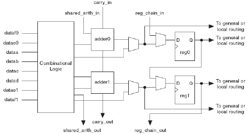
Figure 4: ALM of the Startix-II Courtesy Altera
Each ALM comprises two programmable registers, two dedicated full adders, a carry chain, a shared arithmetic chain, and a register chain.
The Memory module of the Stratix-II device has a TriMatrix memory structure; it includes 3 different kinds of embedded RAM blocks. TriMatrix memory includes M512 blocks, 4KB, M4K blocks and 512KB M-RAM blocks, each of which can be configured to support various features.
The DSP block structure is optimized & configure to achieve multiple DSP functions with maximum performance and minimum logic resource utilization. The DSP blocks of the Xilinx and Altera FPGAs are almost having the same functionalities to perform addition and multiplication operation with minimum latency.
Stratix-II devices come up to 12 phase-locked loops (PLL) and 48 independent system clocks, acting as a central clock manager to meet the system’s timing requirements.


