
Voltage Booster
16/11/2021, hardwarebee
Anyone that ever worked with electronics knows how wide the range of rated voltages in the market is. For example, inside a computer there are at least three different voltage supply lines: 12 V, 5V and 3.3 V. They are needed because the rated voltages of different components, such as processors, fans and hard disks, are inherently different: they vary with the application, brand and model. In this scenario, voltage converting systems are fundamental. Their job is to convert an input voltage (for instance, the main line) to a DC value that can be used by the component. Changing the supply level is the easy part; the problem is doing it in an efficient way, which is why there are so many topologies of power converters. In this article, we will discuss the voltage booster, or boost for short. This circuit is a switched-mode power supply (SMPS) able to output a voltage higher than its input, with the actual value being defined by the duty-cycle of the control signal. We will present the voltage booster basic concepts, the operation modes and some design guidelines, without going too deep into the mathematics of the circuit.
Basic Concepts
Switched-mode power supplies (SSPS) are circuits that combine switching devices, typically field-effect transistors, with reactive components, such as inductors and capacitors, to convert a voltage value efficiently. They are designed to avoid any resistive component that can contribute to power loss. By controlling the flux of power, the output voltage can be adjusted, in a similar way that an on/off pumping system can set the water level in a container. This control is obtained through the duty-cycle of the switching signal, which is used to drive the transistors. To better understand the mechanisms behind the boost, let us look at the circuit in Figure 1.
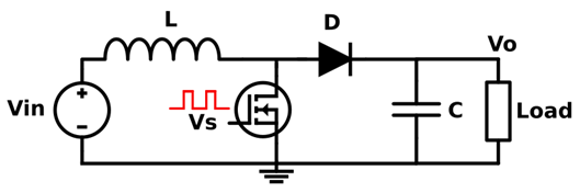
Figure 1: The Basic Boost Converter
There are several ways to analyze this circuit. For now, we will focus on the steady-state operation, so we are going to disregard the transient period, for simplicity. The operation can be divided in two states: switch on and switch off. When the switch is on, we get the following circuit:
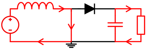
Figure 2: Switch ON State
In this state, the input voltage source transfers energy to the inductor, which is stored as a magnetic field. The characteristic equation of the inductor states that the voltage is proportional to the derivative of the current, so the inductor current is a ramp with a slope defined by the inductance and the input voltage. Meanwhile, the diode is reversed polarized, so it isolates the inductor from the load. The capacitor is responsible for maintaining the output voltage. As we are analyzing the steady-state operation, we consider that the capacitor is already fully charged. During the ON period, the capacitor discharges, with the slope being proportional to the RC time constant. Therefore, the voltage ripple is proportional to the power demand, the capacitance and the ON period. The voltage value across the load is simply:
Vload = Vc
After tON, the control signal opens the switch, which results in the circuit showed below.
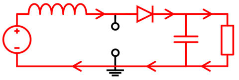
Figure 3: Switch OFF State
The energy stored in the inductor’s magnetic field prevents the current from changing abruptly, so the voltage across its terminals instantly inverts and scales to keep the current value and direction. At this point, the potential difference across the load is equal to:
Vload = Vin + Vl – Vd
During this stage, the stored magnetic energy will be discharged and the inductor current will drop, with a slope proportional to the difference between the input and output voltages. The capacitor will be charged by part of this current, recovering the initial voltage from the previous stage. After tOFF period ends, the circuit goes back to Figure 2. We can then qualitatively state the following:
- To obtain a voltage higher than the input, the boost converter uses the inductor property of not allowing abruptly changes in current;
- The switch ON state is used to charge the inductor, transferring energy to the magnetic field;
- The capacitor and the diode are used to keep the output voltage value with low ripple during the ON state;
- The OFF state transfers the energy from the inductor to the load. To keep the current value, the voltage difference across the inductor inverts its polarity and adds to the input voltage, boosting the total level.
- The combination VIN + VL also charges the capacitor during the OFF
Operation Modes
Continuous Mode
The boost converter can operate in two different ways: the continuous and the discontinuous modes. In the continuous conduction mode (CCM), the tOFF period is small enough to prevent the inductor current to be reach zero. The Figure 4 illustrates the current waveform during continuous operation.
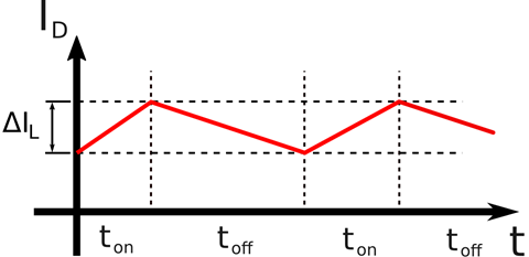
Figure 4: Boost Operating at Continuous Mode
There are several advantages (and disadvantages) of operating in the continuous mode. The first advantage is the calculation simplicity: the output voltage can be evaluated by simply considering that the DC voltage across the inductor must be 0 (otherwise, the current would grow indefinitely). Using this reasoning, and considering the ripple very low so that the output voltage can be considered DC, we find the following equation:
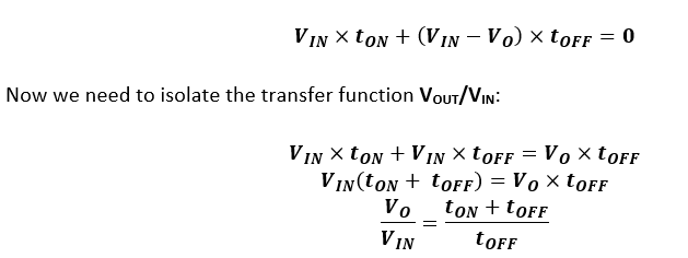
Now, considering a fixed switching frequency fs, let us rewrite the transfer function using the duty-cycle (D = tON/ tS)as independent variable:
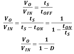
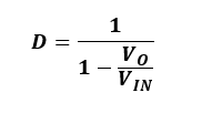
Therefore, in the continuous mode, the output volage can be controlled by the duty-cycle using the equation above. For instance, using a duty-cycle of 50%, the output voltage is two times the input. Notice that Vout is directly proportional to the duty-cycle, and that the equation is highly non-linear. We can rearrange the equation to design a duty-cycle for a defined output voltage:
Discontinuous Mode
If the inductor current reaches zero before the system switches the state, then the circuit enters the discontinuous mode (DCM). This state is much more difficult to analyze, because the “dead-zone” period between the current reaching zero and the switching is also dependent on the duty-cycle. Therefore, the voltage calculation process is completely different.
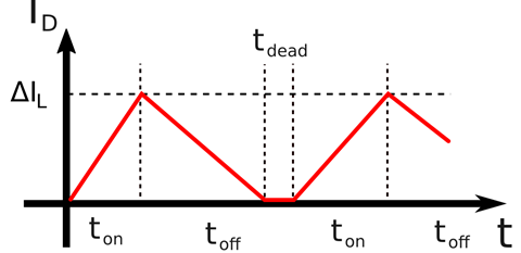
Figure 5: Booster Operating at Discontinuous Mode
To avoid diving too deep into the mathematics, which is not the objective of this article, we are going to left the derivation of the transfer function to the reader. Tip: calculate the average diode current from the inductor current. The average diode current is equal to the average load current, as the DC capacitor current must be zero in steady-state. The output voltage of the booster in discontinuous mode is:
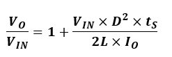
Notice that this equation is much more complicated than the continuous case. Firstly, the relationship with the duty-cycle is quadratic. Secondly, the output voltage depends on several different parameters besides D: the inductor L, the input voltage, the commutation period ts, and the output current IO.
Continuous versus Discontinuous
Both modes can be used, but the continuous mode presents several advantages over the discontinuous. Firstly, the transfer function is simpler, and depends only on the duty-cycle. The DCM transfer function, on the other hand, depends widely on the component values, as well as the load demand, which is not desired in open-loop operation. Moreover, the higher current ripple also increases output noise and current efforts of the components. However, DCM provides lower commutation losses, because the ON switching is performed with zero current, and smaller inductors, as the maximum inductance of DCM is lower than the minimum L required for CCM. Furthermore, the DCM dynamics provides better stability in closed-loop operation, due to the non-minimum phase dynamics of the CCM.
Design Considerations
Inductor
The inductor value controls the current ripple. As explained previously, one can even choose between CCM and DCM by selecting the right inductor. Therefore, the required inductor value in a boost converter is defined by the desired current ripple. By analyzing the first slope of the current waveform in Figure 4, we find the following equation:
By isolating L we find the required inductor:
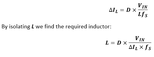
Besides the inductance, the component must withstand the current efforts required. Use the maximum RMS current to select the wire gauge. Moreover, inductor losses must be minimized to maximize efficiency.
Capacitor
The capacitor controls the output voltage ripple of the circuit, similarly to the inductor controlling the current ripple. The relationship between voltage ripple and capacitance can be obtained by calculating the capacitor current. This current is the same as the diode current minus the average diode current. By integrating the charging/discharging current to obtain the charge variation, one finds the voltage variation (ripple). The voltage ripple is:
By isolating the capacitance, we get:
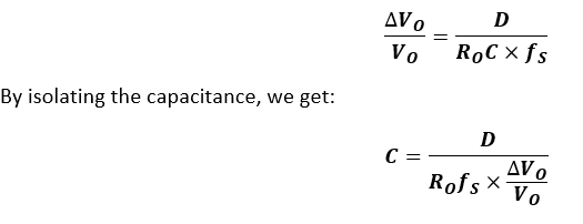
Therefore, if the design required a certain voltage ripple with a load value RO, the capacitance is defined by the equation above. Notice that, by increasing the frequency or decreasing the duty-cycle, the value of the capacitor decreases. Besides voltage ripple, the capacitor must withstand the output voltage. Also, the parasitic resistances should be minimized to avoid losses and complicated dynamics, so capacitors with low ESR should be selected.
Switch
The switch is the heart of the boost converter, so special attention should be paid to it. Firstly, the maximum current should support the inductor peak current (two or three times higher), while the rated voltage should be higher than the maximum output voltage (approximately 1.5 times larger). Secondly, fast switching speed improves both the dynamics and the efficiency of the device, so fast turn-on and turn-off times are desirable. Efficiency also rises with the decrease of the ON resistance. Power MOSFETs are known for their low series resistance, so they are a great choice. However, both input and output capacitances also increase the commutation losses, and MOSFETs with small ON resistance typically have large capacitances. Therefore, there is a trade-off that must be analyzed before component selection. Furthermore, large capacitances mean high gate currents, which affects the driving circuit.
Diode
In boost converters, low forward drop and fast turn-on time are required, to reduce conduction losses and improve the dynamics. Schottky diodes are a good option. The maximum repetitive current be higher than the peak inductor current, whereas the average rated current should consider the mean value of the diode current during conduction. Moreover, the maximum reverse voltage must be higher than the desired output voltage minus the input. Parasitic components, such as ON resistance and capacitance, as well as the reverse recovery current should be minimized.
Synchronous Boosts
The synchronous boost converter is a variation of the simple boost that replaces the diode with a complementary switch. In the ON state, the synchronous switch opens, isolating the load from the inductor similarly to the diode in reverse bias. In the OFF state, the synchronous switch closes, acting as the diode in forward bias. The main advantage of this modification is the reduction in conduction dissipation. Diode conduction losses are caused by the forward voltage VD, which is typically 0.7 V, but can be reduced to 0.2 V. A switch, on the other hand, has a ON resistance in the order of mΩ. This reduces drastically the conduction losses in high current applications. However, complexity is increased due to the complementary control, that must also prevent that both switches are ON at the same time.
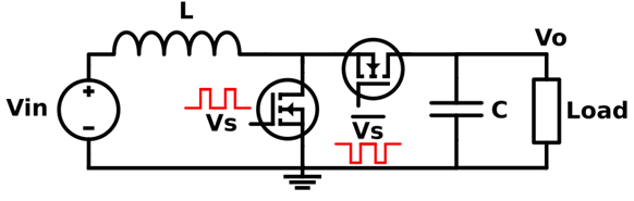
Figure 6: The synchronous boost converter


