• Get Listed
    • Get a FREE Quote for your Next Project
HardwareBee
https://promwad.com/
  • Find ASIC Vendors
  • Browse Design Services Directory
    • FPGA Design Services
    • Electronic Design Services
    • Embedded Software Companies
    • Add a Vendor
  • Get 5 Quotes From
    • FPGA Design Companies
    • Electronic Design Companies
    • Embedded Software Companies
    • Design & Manufacturing Vendors
  • WikiBee
  • Resources
    • FPGA Academy
    • Embedded Academy
    • FPGA vs ASIC Calculator
  • Get Free Consulting
  • Add a Vendor
HardwareBee
  • Browse Design Services Directory
    • FPGA Design Services
    • Electronic Design Services
    • Embedded Software Companies
    • Add a Vendor
  • Get 5 Quotes From
    • FPGA Design Companies
    • Electronic Design Companies
    • Embedded Software Companies
    • Design & Manufacturing Vendors
  • WikiBee
  • Resources
    • FPGA Academy
    • Embedded Academy
    • FPGA vs ASIC Calculator
  • Get Free Consulting
  • Add a Vendor
5727 Views

The Brief Guide to PCB Design Flow

27/04/2019, hardwarebee

A PCB, or a Printed Circuit Board, is one of the most critical components in any electronic product because it is the element that connects all the ICs and passive components that comprises of an electronic product.


If a PCB is lacking one connection, the product will mostly likely not work.


Today, the process of designing and manufacturing PCBs is very robust and consists of a few sequential steps bases on a PC software.


This article is a general overview of the PCB designing process. Some engineers use more (or less) steps in the PCB design flow, but – essentially, all the various PCB design processes are based on the following steps:


Drawing the Schematics


The very first step in the PCB design process is drawing the schematics of the circuit board. You can do so using a schematic capture tool that allows you to create schematics by entering your ICs, passives and connectors into the tool and then connecting all the necessary wires. You can also look into getting a software package that allows you to run simulations. This will let you to test the PCB’s functionality before the manufacturing process.


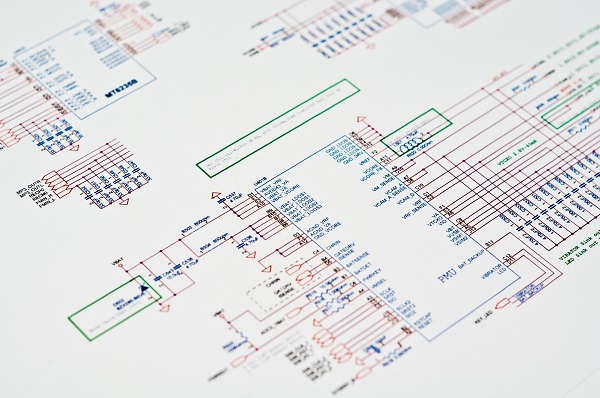
At the end of this step, the schematics are converted into a netlist file. A netlist file is basically a database that has taken your circuit diagram and condensed all the graphic information into a list of nets. Every net represents a wire on the PCB and its connection to the designated components.


PCB Placement


The next step in the PCB design process is to decide about the components (ICs, passives, connectors, etc.) location across the PCB. You will be roughly arranging them on your board to determine that you have enough space and can accommodate the needed elements the way you want. After obtaining a rough placement, you can further look into detailing out the specifics regarding the orientation and the exact positions of each component depending on the number of nets, thermal consideration and other requirements your product may have (for example: antenna location or power supply input etc.).


PCB placement


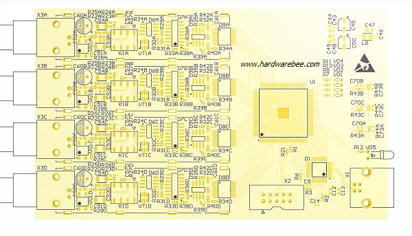
The final placement will be fine-tuned in the routing phase.
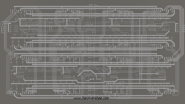
 

PCB Routing


The next step is to determine the route and paths that your interconnections will be taking to get from one pin to another or from one component to another. Routing is generally a time-consuming process as the software takes the information you provided and the netlist to map out the routes on the circuit board across the various layers that you have defined. Some of the nets should be short (for example: clock signals) or equal in length (for example: differential pairs) – you should begin your routing process with the high priority signals.


PCB routing


Design Rule Check


PCB layout software allows you to check whether your PCB can be manufacture by the PCB manufacturing company. Every manufacturing company has various design rules that they provide to PCB designers. The design rule check allows you to detect any discrepancies early on and correct any errors that may potentially cause you trouble in the PCB manufacturing phase. Such error could be: two ICs are too close to each other so that the assembly machine will not able to reach out and place on of them on the PCB.


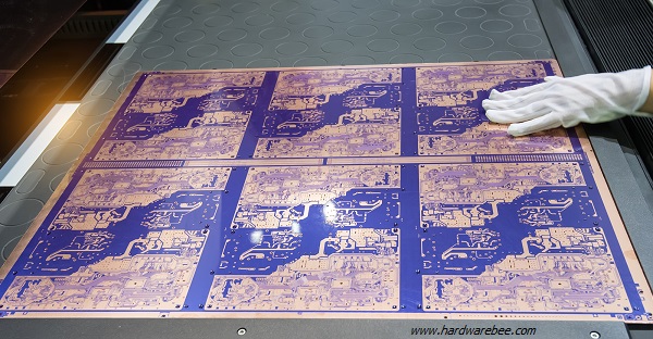
At the end of this process, you will most likely have Gerber files, a standard format for files pertaining to PCBs, containing the visual information and the visual plots for your circuit. Not only do these files contain visual images, but also information regarding the drilling and assembly instructions.


PCB manufactering

linked in icon
Sign up for HardwareBee
* = required field

Recent Stories

What is the Principle of an Electric Motor
Introduction to Thyristors
Top Three Suppliers Held 94% of 2021 DRAM Marketshare
Understanding Full-Wave Rectifiers
Working Principle of a Transformer
Understanding Quiescent Current
Understanding Transimpedance Amplifier
Understanding Sample and Hold Circuit
Get 3 Quotes from Electronic Design Companies
Get 3 Quotes from FPGA Design Companies
Get 3 Quotes from Embedded SW Services
Get 3 Quotes from EMS Companies

Find Design Services

Get Price Offers From
  • Electronic Design Services
  • FPGA Design Services
  • Embedded Software Companies
  • PCB Layout Services
  • Printed Circuit Board Manufacturers
  • Design & Manufacturing Services
Welcome New Vendors
  • IDW Innovation Studio
  • Micro Technology Services
  • Byte Lab
  • Orthogone Technologies
  • Faststream Technologies
Answer a Question
  • Tips For Installing a PCB Prototype Board
  • Benefits of Working With a Reliable Flex Printed Circuit Board Manufacturer
  • FPGA company gross margin?
  • What is an FPGA used for?
  • When was FPGA invented
Recent WikiBee Items
  • FPGA Ethernet Overview
  • Flyback Converter
  • FPGA FFT Overview
  • Inverting Op Amp
  • FPGA Logic Analyzer
Recent Posts
  • What is the Principle of an Electric Motor
  • Introduction to Thyristors
  • Top Three Suppliers Held 94% of 2021 DRAM Marketshare
  • Understanding Full-Wave Rectifiers
  • Working Principle of a Transformer
Most Popular Blog Posts
  • Embedded Academy
  • Firmware and Embedded Software Development Services
  • IoT Software Development Company
  • Embedded Software Company
  • Firmware Development

Never miss an update!

Follow us on LinkedIn

Do you need any price
information?

(Electronic design, FPGA design, Embedded SW services, PCB design, Turnkey)

Yes
No
HardwareBee

Copyright 2017-2022, HardwareBee. All rights reserved.

  • About Us
  • Contact
  • Subscribe
  • News
  • Get Free Support
  • Get listed
  • Send a wiki/article
  • Advertise

Follow Us

Be sure to follow our LinkedIn company page where we share our latest updates LinkedIn
Partner with us Partner with us

Design and Manufacturing Services

  • Engineering Design Services
  • Electronic Design and Manufacturing
  • Electronic Product Development
  • Electronic Product Design
  • Electronic Consulting Services
  • Electronic Engineering Companies
  • Electronic Engineering Services
  • Electronic Product Design and Development
  • Electronics Design Services
  • Electronics Design Company
  • Electronic Design Consultants
  • Electronic Design Company
  • FPGA Design Company
  • FPGA Consultant
  • FPGA Design Services UK
  • Electronics Manufacturing services
  • Electronics Manufacturing Companies
  • Electronic Contract Manufacturing Companies
  • Electronic Manufacturing Services Companies
  • EMS Companies Directory
  • Electronic Design Services
  • FPGA Design Services
  • Embedded Software Companies
  • PCB Layout Services
  • Printed Circuit Board Manufacturers
  • Design and Manufacturing Services