The Ultimate Guide to FPGA Design
30/05/2021, hardwarebee
This article provides an overview of FPGA design. FPGA design is today a very mature process that as evolved since the 80’s. Of course, new development tools have been developed and FPGAs got larger and larger to resemble an SoC (System on a Chip). But, the general concept of FPGA design is still very similar to the original one.
Usually, FPGA design is created with hardware description languages such as Verilog and VHDL. These languages provide a discrete event computer model that generates hardware. These languages are used to create synchronous design. Discrete-event models are commonly used in the modeling of complex systems.
How to Design FPGA
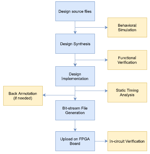
The basic steps involved in FPGA design are listed in figure below. Where everything starts from idea development, then the idea is transformed to a code. The code is then simulated and debugged for functional verification. After all the verifications, the code is ready to download into the FPGA.
FPGA Design Flow
Figure 1 depicts the primary five stages in the FPGA design process. The five main steps are Functional Design, Synthesis, Place & Route, Integration, and Fabrication. Each stage, contains a complete generate-simulate cycle in which the design components are generated and then simulated to ensure appropriate functioning before moving on to the next stage. The parts that follow will go through each of these processes in greater depth.
FPGA Functional Design
The process of turning an original system concept into an actual FPGA implementation that accomplishes the needed tasks is known as functional design. The basic concept for the design cycle must specify how the design will be partitioned among various FPGAs if necessary.
The process of functional design starts with the formation of a description of a system’s sections (building blocks) in the most natural way feasible for the component in question. The simplest description methodology for fundamental structures built from primitive Actel, such as Multi-bit registers and multiplexors, is schematic capture using Design Architect (DA).
For blocks containing random programming, such as decoders or ALUs, the easiest explanation is typically a hand-generated synthesizable VHDL model. Although automated HDL generators such as Renoir may be used to construct the natural graph description of a VHDL model, the simplest description is also a Synthesizable VHDL model for Finite State Machines (FSMs), such as controllers.
After the building blocks have been first described, they should be separately simulated to check that they are properly functioning. This is done using the model-simulator, schematic Quicksim or VHDL model ModelSim. The building block construction and simulation flows are illustrated in Figure 2. Be aware that the Actel preimvpt tool must be used in the production, prior to simulation with Quicksim, of a unit delay simulation point for schemes constructed using Actel Library elements.
The next stage is to construct the RTL-level Datapath using the building blocks, once each of the building blocks has been developed and simulated. Building blocks and any extra components of the Actel library are connected in the RTL level data track and therefore this phase with schematic capture is most effectively handled using Design architect again.
Before they can be used in a system devised by the architect, they must have symbols assigned to them. This is simple to accomplish in Design Architect for both schematic and VHDL blocks. Following the definition of the symbols, the design architect may be used to develop the overall design structure by connecting building blocks into a pattern. After completing this stage, the complete design should be functionally simulated once again to confirm correct operation.
It should be noted that simulations may be conducted frequently as the concept is developed that helps to isolate problems as they occur. For example, the Simulator Force files may be used to drive the control points to assure appropriate operations, to replicate the data flow, without the control system first. It will then be possible to add the controller model and simulate the resulting design. Finally, it is possible to add I/O pads and any additional logic, such reset generator or glue logic to imitate the entire design (typically a whole FPGA).
Automatically, Design Architect will incorporate all attributes necessary when building VHDL symbols for Flexsim models to simulate VHDL models using Quicksim components. Flexsim is a backplane for simulation that connects Quicksim and ModelSim and accesses the tool through QSPro. When the QSPro tool is used to simulate Quicksim components with VHDL models, an issue exists; the combination does not handle simulations with zero delays. If no delays are introduced to the control outputs of the FSM VHDL model, it is exceedingly difficult to determine the sequence of events in the following clock cycle.
If it were the worst case, the simulation would fail because the events appear in an acceptable sequence at zero time (a complete VHDL simulation would not have this problem since it has been specifically created with a delta delay mechanism by VHDL to manage it). The allocation of outputs in all VHDL-models can also be postponed by a few nanoseconds. This may be done by means of handmade VHDL behavioral models or Renoir models. Due to such delays, it is much easier to ignore the functional simulation technology during the synthesis phase. The design flow for functional design RTL is shown in Figure 2.
FPGA Synthesis
The mapping of VHDL computational models into logical gate implementations is known as synthesis. The Exemplar tool of Leonardo Spectrum, which is part of the Mentor Graphics tool package, is used for synthesis. Leonardo Spectrum is a synthesis tool for FPGAs. Input and output that comprises a net-list of library components of the specified technology, in this case the Actel ACT1 family. VHDL or Verilog accepts the data. EDIF (Electronic Design Interchange Structure), VHDL, Verilog or XNF can format output netlist format (a netlist format specifically for Xilinx FPGA tools). The EDIF outcome format is utilized for this design flow and may be sent back to the Mentor Graphics environment simply.
One of the essentials in the synthesis process, of course, is the start of the functional design process by writing synthesizable models of VHDL. Because VHDL is a high standard language, it has a lot of complicated constructions that allow for modeling in different styles (such as recursion) but are nonsensical and hence are not synthesizable for real hardware implementation.
Fortunately, the Renoir tool generates synthesizable code for state machines, so the behavioral descriptions provided by hand may be synthesized for the random logical blocks. Although the basic VHDL descriptions may be synthesized, the Leonardo Spectrum tool requires a number of synthesizable VHDL books and references, including an HDL Synthesis Guide that specifies the VHDL subset and code-style. If there are any doubts about the synthesizability of a VHDL model using Leonardo Spectrum, this reference should be checked.
When the VHDL code is generated in the Actel library component at gate level implementation, it is reimported for simulation verification and export to the Actel toolset into the Mentor Graphics environment. Actel is the so-called edn2mgc tool which takes the EDIF netlist output from Leonardo Spectrum and produces a design that fits into the Design Architect scheme and the Quicksim simulation in Mentor Graphics database format.
Because it is a netlist format without an internal system, it is impossible to analyze an internal structure created by synthesized tools or to trace internal signals in the simulation block within a Synthesized Block. Designers desire the Schematic Creations Tool of Mentor Graphics to build out a scheme for the synthesized block before they can be merged with the overall design, but this is not always essential.
Once the VHDL blocks are synthesized, new symbols must be produced to them (as now schematics instead of VHDL models). The synthesized blocks instead of VHDL models have to be used to create a new overall RTL level schematic. It is an easy technique to do that to save the original RTL level design, which included the VHDL models and edit it to remove the VHDL blocks and replace them with their synthetic counterpart. The whole design will be in the Actel library components after the schematic is finalized.
At this stage it is vital to recreate this design functionally to make sure it is proper in advance. The presimvpt tool again creates the correct unit delay point for the simulation and is utilized for the simulation by the Quicksim simulator. The design flow for the synthesis phase is shown in Figure 4.
FPGA Place and Route
The design is inserted and routed to Actel FPGA after completion of the synthesis procedure and functional simulation of the completely executed design. The designer must divide the design, as previously said, into FPGAs because the tools from Actel are not automated. Therefore, if more than one FPGA is involved in the design, the designs submitted in the location and route tool must reflect the one FPGA component of the whole design. All design inputs, outputs and bidirectional (three-state) input/output signals should also have Actel I/O pads on it.
Figure 5 shows the location and route design stream that begins when the full design is established and routed with the development of an EDIF net list. This method uses the Actel mgc2edn tool. After the establishment of the EDIF List, the Actel Designer tool is utilized for the actual place and route tasks. Designer uses an internet list format to read, complete, insert and route the EDIF file and then produce a time file that can be backed into the Mentor Graphics environment for extensive timing simulations of the final FPGA implementation.
Note that the kind and size of Actel FPGA to be inserted in the initial compilation step by the user in the Designer must be specified. In the course of compiling, the Designer checks for the right design using Actel components (e.g. no internal I/O pads, no fanout breaches, etc.) and first checks to ensure that the design fits the specified FPGA. Nevertheless, it is important to remember that a completed compilation procedure successful does not allow the designer tool to install the design and transfer it to the FPGA of choice.
Many aspects, including the design structure and regularity, the quantity of inputs and outputs in the design, impact whether a successful placement and routing is possible. Uses using just 60 percent of the available FPGA logic modules were not totally installed and routed, while in more than 90 percent of the cases other designs were effectively finished.
The Actel del2mgc Tool is used to import it back into the mentor graphics environment once the timing information is set, routed and extracted in the Designer tool. As a result, it is a good idea to recreate the design of the chip level via a standard time-changer to make sure each chip works correctly at the selected clock speed with genuine delays.
FPGA Integration
The penultimate step is termed system integration before the real design. System integration is constructing and simulating a complete system graph including all FPGAs and other devices, such as EPROMs, PLDs, RAMs, and so on. As far as efficiency is concerned, the model is quite close to the actual system and successful simulation shows that the physical prototype functions well. This is the latest digital prototype stage.
Figure 6 illustrates the system integration flow that starts with the use of Design Architect to develop symbols for each FPGA schema after completion of placement and routing procedures. The whole system’s schematic is then constructed with the Design Architect. The Mentor Graphics parts library or third-party sources are able to access models for new system components. After the system schemes have been completed, the Design Viewpoint Editor (DVE) Mentor Graphics program must be used to back up the time information for the different FPGAs in the system design.
For each FPGA, the Actel del2mgc tool was used in the placement and routing phase. While the del2mgc tool uses DVE to execute a back annotation, the DVE must directly be utilized to add the appropriate delay information to the whole system simulation for each individual FPGA. Quicksim is used to simulate the delay information using the timing switch, which employs normal time values. The simulations should be reported as thoroughly as possible at this stage in order for any design defects to be identified before the real prototype is created. The amount of simulation performed can, however, be limited to the time required to execute the simulation.
What is HDL Design
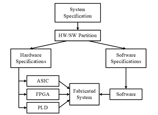
Domains of HDL application is adapted by all the levels of competence. The first step is system specifications, and then the system is divided in two parts, hardware and software. On the hardware side, it can be ASIC, FPGA or PLD (Programmable Logic Device). And for the fabricated system, the software acts as the brain of the hardware and makes it work properly.

The basic limitation of HDL languages is the that it cannot process the analog signals, as it can only deal with digital systems. And the HDL models can be divided in different abstractions like HDL (the highest level of abstraction), then Gate Level, Netlist and Layout (lowest level of abstraction).
The HDL hierarchy can be divided in many different levels as shown in figure below. On left side, we can observe that the top module can be divided in two different sub modules while the sub module can be further sub divided in basic level modules. This can be better understood while comparing this with an example on the right side of figure below.


