
A Practical Guide to FPGA Programming
21/08/2019, hardwarebee
This tutorial outlines the development flow for FPGA programming and presents a simplified example to elaborate FPGA programming in real life. The example is based on Intel’s development board that consists of analog-to-digital converters (ADC) and digital-to-analog converter (DAC).
In this FPGA programming tutorial we will create a simple project that is taking an input signal for ADC from on-board potentiometer and outputs to user LEDs and DAC that are also located on the development board. User LEDs and DAC output are changing according to the potentiometer input voltage. Watch the following video to see the demo live.
In this article, we will be using two tools: Quartus 16.0 IDE and Modelsim-Intel together with an FPGA development board for MAX 10 and USB Bluster. MAX 10 development board has two ADCs. The ADCs provide the MAX 10 devices with built-in capability for on-die temperature monitoring and external analog signal conversion.
This FPGA programming tutorial provides all the required steps, instruction and source files to help you get started and to allow you try re-creating this project in your own environment.
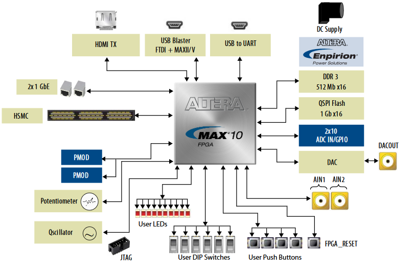
MAX 10 Development Kit is centered around Max 10 FPGA devices from Intel (Altera). The board is used for development and evaluation of the Intel MAX 10 FPGA family and provides well documented hardware platform for beginners in FPGA development.
Step 1: Setting Up the Tools and FPGA Environment
Please note: you can download all the files here.
Let’s start from setting up and simulation the ADC core. In the Quartus Prime Standard Edition start new project, specify working directory (please note – there is shouldn’t be spaces in the name of directory), name of project and select 10M50DAF484C8GES device. Open in the IP catalog Intel Modular ADC core, write entity name adc_core and set settings like shown below:
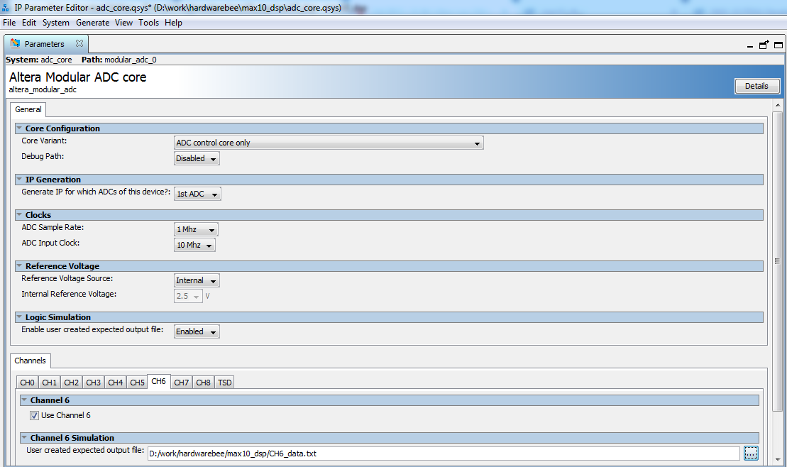
The core variant for 1st ADC is ADC control core only, it allows to control the ADC core directly from the HDL code without soft processor Nios. This enables user created expected output file for simulation ADC core. Set only one channel – number 6, that is tied to potentiometer on the development kit. Point to user expected output file (in my case is CH6_data.txt). File CH6_data.txt consist information about step and voltage are going to apply to ADC channel:
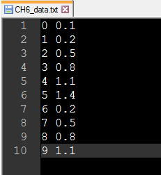
The left column is used for arranging voltage Vin that is taken from right column. There is space between two columns. The output of ADC core will be computed like Vin \ 2.5 V * 4096 [2].
Now, generate the ADC core and check create simulation model before. Manually add adc_core.qip, adc_core.sip and adc_core.qsys files into project. Create top-level Verilog file max10_dsp.v with ADC and ALTPLL IP cores included:
`timescale 1 ns / 1 ns
module max10_dsp (
//Reset and Clocks
input CLK_50_MAX10, //2.5v
input CLK_10_ADC, //2.5v
input CPU_RESETn,
// DAC
output DAC_SYNC, //3.3-v LVCMOS
output DAC_SCLK, //3.3-v LVCMOS
output DAC_DIN, //3.3-v LVCMOS
output [4:0] USER_LED
);
wire [4:0] command_channel = 5’d6;
wire command_ready;
reg [4:0] leds_reg = 5’b11111;
wire locked;
wire clk10MHz;
wire response_valid;
wire [4:0] response_channel;
wire [11:0] response_data;
always@(posedge CLK_50_MAX10)
if(response_valid && response_channel == 5’d6) leds_reg <= response_data[11 : 7];
pll_clock u0 (
.inclk0 ( CLK_50_MAX10 ),
.c0 ( clk10MHz ),
.locked ( locked )
);
adc_core u1 (
.clock_clk (CLK_50_MAX10), // clock.clk
.reset_sink_reset_n (CPU_RESETn), // reset_sink.reset_n
.adc_pll_clock_clk (clk10MHz), // adc_pll_clock.clk
.adc_pll_locked_export (locked), // adc_pll_locked.export
.command_valid (1’b1), // command.valid
.command_channel (command_channel), // .channel
.command_startofpacket (1’b0), // .startofpacket
.command_endofpacket (1’b0), // .endofpacket
.command_ready (command_ready), // .ready
.response_valid (response_valid), // response.valid
.response_channel (response_channel), // .channel
.response_data (response_data), // .data
.response_startofpacket (), // .startofpacket
.response_endofpacket () // .endofpacket
);
assign USER_LED = leds_reg;
endmodule
The IP core ALTPLL should be added to project for generating clock and locked signals to ADC. Settings of ALTPLL IP core is: 50 MHz input clock, unchecking areset signal, the output clock frequency is 10 MHz. Now, run Analysis and Synthesis.
The project’s working directory consists of folder adc_core with all necessary files for simulation ADC IP core except testbench file. So — there is quite simple testbench file that describes behavior of ADC core inputs as follows:
`timescale 1 ps / 1 ps
module adc_core_tb();
reg clk50MHz;
reg clk10MHz;
reg locked;
reg reset_n;
reg command_valid;
reg [4:0] command_channel;
reg command_startofpacket;
reg command_endofpacket;
wire command_ready;
wire response_valid;
wire [4:0] response_channel;
wire [11:0] response_data;
wire response_startofpacket;
wire response_endofpacket;
adc_core u0 (
.clock_clk (clk50MHz), // clock.clk
.reset_sink_reset_n (reset_n), // reset_sink.reset_n
.adc_pll_clock_clk (clk10MHz), // adc_pll_clock.clk
.adc_pll_locked_export (locked), // adc_pll_locked.export
.command_valid (command_valid), // command.valid
.command_channel (command_channel), // .channel
.command_startofpacket (command_startofpacket), // .startofpacket
.command_endofpacket (command_endofpacket), // .endofpacket
.command_ready (command_ready), // .ready
.response_valid (response_valid), // response.valid
.response_channel (response_channel), // .channel
.response_data (response_data), // .data
.response_startofpacket (response_startofpacket), // .startofpacket
.response_endofpacket (response_endofpacket) // .endofpacket
);
always #20 clk50MHz = ~clk50MHz;
always #100 clk10MHz = ~clk10MHz;
initial begin
clk50MHz = 0;
clk10MHz = 0;
reset_n = 0;
locked = 1;
command_valid= 1;
command_channel = 5’d6;
command_startofpacket = 0;
command_endofpacket = 0;
# 1000;
reset_n = 1;
# 100;
locked = 1;
# 50000;
$stop;
end
endmodule
The Modelsim-Intel tool will be used for simulation of the ADC IP core therefore it’s necessary to create a launch script .do file. For creating a launch script go to mentor folder situated into adc_core/simulation folder. There is a Quartus generated msim_setup.tcl script file that is used for creating Modelsim-Intel launch file. From msim_setup.tcl take only the part between # # TOP-LEVEL TEMPLATE – BEGIN and # # TOP-LEVEL TEMPLATE – END strings and edit like this:
# # TOP-LEVEL TEMPLATE – BEGIN
# #
# # QSYS_SIMDIR is used in the Quartus-generated IP simulation script to
# # construct paths to the files required to simulate the IP in your Quartus
# # project. By default, the IP script assumes that you are launching the
# # simulator from the IP script location. If launching from another
# # location, set QSYS_SIMDIR to the output directory you specified when you
# # generated the IP script, relative to the directory from which you launch
# # the simulator.
# #
set QSYS_SIMDIR .
# #
# # Source the generated IP simulation script.
source $QSYS_SIMDIR/mentor/msim_setup.tcl
# #
# # Set any compilation options you require (this is unusual).
# set USER_DEFINED_COMPILE_OPTIONS <compilation options>
# #
# # Call command to compile the Quartus EDA simulation library.
dev_com
# #
# # Call command to compile the Quartus-generated IP simulation files.
com
# #
# # Add commands to compile all design files and testbench files, including
# # the top level. (These are all the files required for simulation other
# # than the files compiled by the Quartus-generated IP simulation script)
# #
vlog -vlog01compat -work work submodules/adc_core_modular_adc_0.v
vlog -vlog01compat -work work submodules/Intel_modular_adc_control.v
vlog -vlog01compat -work work submodules/Intel_modular_adc_control_avrg_fifo.v
vlog -vlog01compat -work work submodules/Intel_modular_adc_control_fsm.v
vlog -vlog01compat -work work submodules/chsel_code_converter_sw_to_hw.v
vlog -vlog01compat -work work submodules/fiftyfivenm_adcblock_primitive_wrapper.v
vlog -vlog01compat -work work submodules/fiftyfivenm_adcblock_top_wrapper.v
vlog -vlog01compat -work work adc_core.v
vlog -vlog01compat -work work adc_core_tb.v
# #
# # Set the top-level simulation or testbench module/entity name, which is
# # used by the elab command to elaborate the top level.
# #
set TOP_LEVEL_NAME adc_core_tb
# #
# # Set any elaboration options you require.
# set USER_DEFINED_ELAB_OPTIONS <elaboration options>
# #
# # Call command to elaborate your design and testbench.
elab
# #
# # Run the simulation.
add wave *
view structure
view signals
run -a
# #
# # Report success to the shell.
# exit -code 0
# #
# # TOP-LEVEL TEMPLATE – END
Save it into modelsim_script.do file. This file consists of information about ADC IP core files for simulation in Modelsim-Intel tool and may be used separately without Quartus software. Now, open created modelsim_script.do by modelsim.exe application. In the command line run do modelsim_script.do command, it allows to run testbench for ADC IP core. The Wave simulation looks like this:
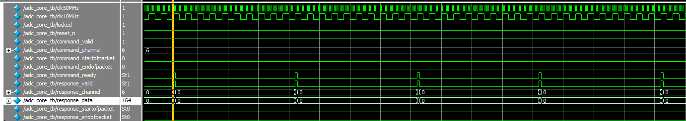
Signal command_valid always high, signal command_channel is set to 6, wire response_channel is 6 and response data is 164, 328, 819, 1311 and so on, the data is set according voltage being write down in CH6_data.txt (0.1/2.5 * 4096 = 164, 0.2/2.5*4096=328 and so on).
The majority of Intel IP cores could be simulated in such manner. That is good starting point for using IP cores.
The DAC component of the development kit is represented by Texas Instrument DAC8551 microchip [3]. One has three wire input that is compatible with standard SPI interfaces, a diagram for SPI serial write operation is shown below:
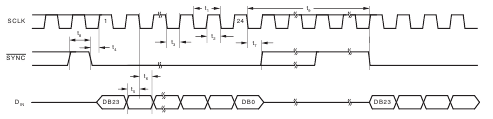
The write operation is provided by asserting to low SYNC signal and SCLK clock up to 30 MHz, 24 bits of data is clocked on falling edge. A simple finite state machine (FSM) for developing DAC driver will be used for this tutorial. When writing any HDL code it’s recommended to use for reference Recommended HDL Coding Styles [4] or templates that can be found in Quartus software. This ensures the FPGA developer that all basic elements (trigger, latch, ROM memory, etc.) will be correctly recognized by the RTL logic by synthesis tool.
A typical FPGA Design Flow consists of:
- Design Entry
- Synthesis
- Implementation
- Program FPGA
Step 2: FPGA Design Entry
Let’s start with inserting a template for Verilog HDL 4-state Moor FSM. Moor FSM outputs are depending only on current state; outputs for DAC are DAC_SYNC, DAC_SCLK, DAC_DIN. HDL code for Moor FSM
// FSM DAC logic
// Declare state register
reg [1:0] state;
reg clkDAC = 1’b0;
reg [23:0] shift_reg;
reg [5 :0] half_bit;
reg [11:0] adc_reg;
wire DAC_SYNC_Latch;
// Declare states
parameter Idle = 0,
Wait = 1,
Load = 2,
Feed = 3;
// Determine the next state
always @ (posedge CLK_50_MAX10) begin
if (!CPU_RESETn)begin
state <= Idle;
shift_reg <= 24’d0;
half_bit <= 6’d0;
clkDAC <= 1’b0;
adc_reg <= 12’d0;
end
else
case (state)
Idle: begin
state <= Wait;
clkDAC<= 1’b1;
half_bit<= 6’d0;
end
Wait:
if (response_valid && response_channel == 5’d6)begin
state <= Load;
adc_reg <= response_data;
end
else
state <= Wait;
Load: begin
shift_reg <= {8’h00, adc_reg, 4’h0};
state <= Feed;
clkDAC<= 1’b1;
half_bit<= 6’d0;
end // Load state
Feed: begin
if(half_bit == 6’d47)
state <= Idle;
else
state <= Feed;
clkDAC <= ~clkDAC;
half_bit <= half_bit + 6’d1;
if(half_bit[0]) shift_reg <= {shift_reg[22:0], 1’b0};
end // Feed state
endcase
end
reg DAC_SYNC_lt;
reg DAC_SCLK_lt;
reg DAC_DIN_lt;
// DAC Outputs depend only on the state
always @ (state or clkDAC or shift_reg[23]) begin
case (state)
Idle: begin
DAC_SYNC_lt = 1’b1;
DAC_SCLK_lt = 1’b0;
DAC_DIN_lt = 1’b0;
end
Wait: begin
DAC_SYNC_lt = 1’b1;
DAC_SCLK_lt = 1’b0;
DAC_DIN_lt = 1’b0;
end
Load: begin
DAC_SYNC_lt = 1’b1;
DAC_SCLK_lt = 1’b0;
DAC_DIN_lt = 1’b0;
end
Feed: begin
DAC_SYNC_lt = 1’b0;
DAC_SCLK_lt = clkDAC;
DAC_DIN_lt = shift_reg[23];
end
default: begin
DAC_SYNC_lt = 1’b1;
DAC_SCLK_lt = 1’b0;
DAC_DIN_lt = 1’b0;
end
endcase
end
// assigments
assign DAC_SYNC = DAC_SYNC_lt;
assign DAC_SCLK = DAC_SCLK_lt;
assign DAC_DIN = DAC_DIN_lt;
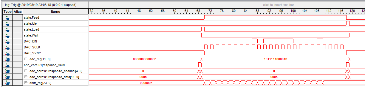
Register adc_reg is used for taking data from ADC 6 channel on response_valid high signal and 24 bit shift register shift_reg is used for moving data in serial on DAC_DIN signal. The FSM state will define level and behavior of DAC_SYNC and DAC_SCLK signals. Counting of bits in shift register is done by half_bit counter.
Step 3: FPGA Synthesis
After the Analysis & Synthesis step, the HDL code will be checked and recognized in RTL logic. The Quartus state machine viewer FSM states will look like this:
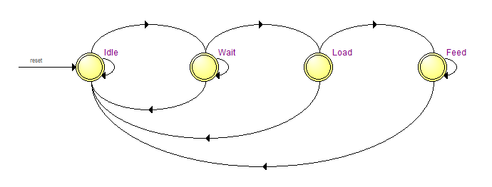
There are 4 states: Idle, Wait, Load and Feed. After reset, the FSM will move to Idle state, where all registers will be initialized. The state Wait FSM will be expecting response_valid signal from ADC on 6th channel. On Load state the shift register will be loaded after getting ADC response_data by adc_reg register. The Feed state provides correct level and behavior of DAC_SYNC, DAC_SCLK and shifting data in shift register. When Feed state finished moving data to DAC FSM it will return back to Idle state and all registers will be reinitialized.
Functional simulation is performed on the synthesis step. This kind of simulation doesn’t consider timing requirements. Now, the entire project with ADC/DAC can be simulated with testbench. It will look like this:
`timescale 1 ps/ 1 ps
module max10_dsp_vlg_tst();
// reg CLK_10_ADC;
reg CLK_50_MAX10;
reg CPU_RESETn;
// wires
wire DAC_DIN;
wire DAC_SCLK;
wire DAC_SYNC;
// assign statements (if any)
max10_dsp i1 (
// port map – connection between master ports and signals/registers
// .CLK_10_ADC(CLK_10_ADC),
.CLK_50_MAX10(CLK_50_MAX10),
.CPU_RESETn(CPU_RESETn),
.DAC_DIN(DAC_DIN),
.DAC_SCLK(DAC_SCLK),
.DAC_SYNC(DAC_SYNC)
);
always #20 CLK_50_MAX10 = ~CLK_50_MAX10;
initial
begin
CLK_50_MAX10 = 0;
CPU_RESETn = 0;
# 1000;
CPU_RESETn = 1;
# 150000;
$stop;
$display(“end simulation”);
end
endmodule
The signals CLK_50_MAX10 and CPU_RESETn are set and ADC will be useing input analog signals defined in CH6_data.txt file. Simulation results are shown below:
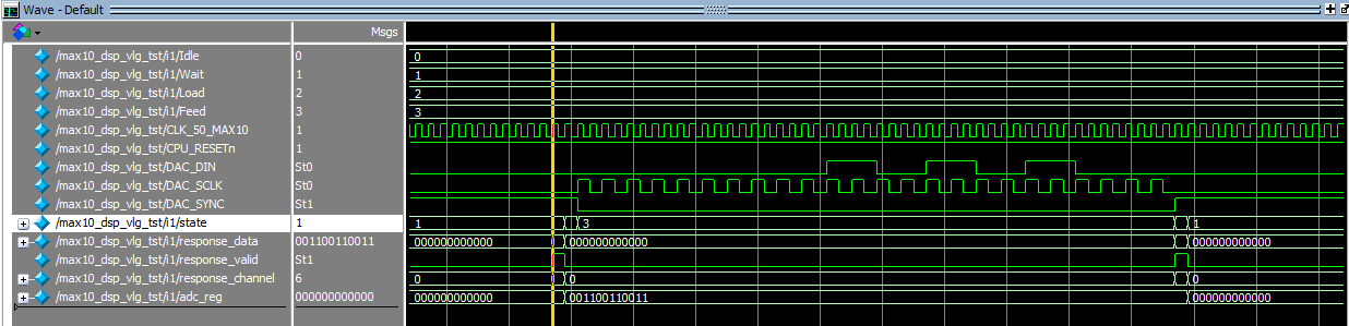
The Project simulation allows debugging the behavior of FSM for DAC data serialization. After simulation, a pinout assignment is needed. All pinout will set according MAX10 development kit user guide. Assignment may be found in max10_dsp.qsf file and for outputs look like this:
set_location_assignment PIN_M9 -to CLK_50_MAX10
set_location_assignment PIN_D9 -to CPU_RESETn
set_location_assignment PIN_A8 -to DAC_DIN
set_location_assignment PIN_A7 -to DAC_SCLK
set_location_assignment PIN_B10 -to DAC_SYNC
set_location_assignment PIN_AA22 -to USER_LED[4]
set_location_assignment PIN_AA21 -to USER_LED[3]
set_location_assignment PIN_U21 -to USER_LED[2]
set_location_assignment PIN_U22 -to USER_LED[1]
set_location_assignment PIN_T20 -to USER_LED[0]
set_instance_assignment -name IO_STANDARD “1.5 V” -to USER_LED[4]
set_instance_assignment -name IO_STANDARD “1.5 V” -to USER_LED[2]
set_instance_assignment -name IO_STANDARD “1.5 V” -to USER_LED[3]
set_instance_assignment -name IO_STANDARD “1.5 V” -to USER_LED[1]
set_instance_assignment -name IO_STANDARD “1.5 V” -to USER_LED[0]
set_instance_assignment -name IO_STANDARD “1.5 V” -to USER_LED
set_instance_assignment -name IO_STANDARD “3.3-V LVCMOS” -to CPU_RESETn
set_instance_assignment -name IO_STANDARD “3.3-V LVCMOS” -to DAC_SCLK
set_instance_assignment -name IO_STANDARD “3.3-V LVCMOS” -to DAC_SYNC
set_instance_assignment -name IO_STANDARD “3.3-V LVCMOS” -to DAC_DIN
Step 4: FPGA Implementation
Before starting the Implementation phase, it’s needed to add signals by using the Signal tap. This tool allows debugging the design after place and route the project into an FPGA. Same signals are used in the functional simulation. After Implementation and Program FPGA Signal tap tool is used for debugging the project directly into FPGA.
Step 5: FPGA Programming and Results
The results of debugging after implementation are the same as in the functional simulation. A very important step was missed in this tutorial ‑ timing analyze. This step should be done if project is very large or\and consists of logic for working with fast peripheral like high speed ADC, PCIe, Ethernet and so on.
Please click on the video below to watch the project demo in real life:
References:
- https://www.intel.com/content/dam/www/programmable/us/en/pdfs/literature/ug/ug-max10m50-fpga-dev-kit.pdf
- https://www.intel.com/content/dam/www/programmable/us/en/pdfs/literature/hb/max-10/ug_m10_adc.pdf
- http://www.ti.com/lit/ds/symlink/dac8551.pdf
- https://www.intel.com/content/dam/www/programmable/us/en/pdfs/literature/hb/qts/qts_qii51007.pdf


