HardwareBee
https://www.nuvation.com/
  • Find ASIC Vendors
  • Design Services Directory
    • FPGA Design Services
    • Electronic Design Services
    • Embedded Software Companies
    • Add your company
  • Get Price Quotes From Vendors
    • Electronic Design Companies
    • FPGA Design Companies
    • Embedded Software Companies
    • Design & Manufacturing Companies
    • Get IC Device Prices
  • Emerging ICs Directory
    • UWB
      • Spark Microsystems
    • FPGA
      • Colonge Chip
      • Rapid Silicon
    • Radar
      • Acconeer
    • Add your IC
  • Get IC Prices
  • WikiBee
  • Resources
    • FPGA Academy
    • Embedded Academy
    • FPGA vs ASIC Calculator
    • Watt to dBm Converter
    • dBm to Watt Converter
  • Pricing
    • Get Your Company Listed
    • Book a Demo
    • Get a Monthly Lead List
HardwareBee
  • Design Services Directory
    • FPGA Design Services
    • Electronic Design Services
    • Embedded Software Companies
    • Add your company
  • Get Price Quotes From Vendors
    • Electronic Design Companies
    • FPGA Design Companies
    • Embedded Software Companies
    • Design & Manufacturing Companies
    • Get IC Device Prices
  • Emerging ICs Directory
    • UWB
      • Spark Microsystems
    • FPGA
      • Colonge Chip
      • Rapid Silicon
    • Radar
      • Acconeer
    • Add your IC
  • Get IC Prices
  • WikiBee
  • Resources
    • FPGA Academy
    • Embedded Academy
    • FPGA vs ASIC Calculator
    • Watt to dBm Converter
    • dBm to Watt Converter
  • Pricing
    • Get Your Company Listed
    • Book a Demo
    • Get a Monthly Lead List
8997 Views

PTH Drilling in HDI Circuits

02/07/2018, hardwarebee

Get a Price Quote

Manufacturers now commonly make high density interconnect or HDI boards, as these are the fastest growing technologies. Compared to the traditional circuit boards, HDI circuits have a higher circuit density because fabricators use blind or buried vias and microvias when making the boards.

Manufacturers make six different types of HDI boards with:


  • Double sided PTH with through vias from surface to surface
  • Buried and through vias along with PTH drilling
  • Multiple HDI layers with through vias and microvias
  • Passive substrates without any electrical connections
  • Coreless construction using layer pairs
  • Alternate constructions of coreless constructions using layer pairs

With technology changing according to consumer demand, designers using the HDI technology can now place more components on both sides of the PCB. This is primarily possible because they can use the via-in-pad process that allows more technology on fewer layers. Use of HDI technology allows products to weigh less and be physically smaller. Along with thinner materials and shrinking components, HDI technology is allowing electronics to shrink in size while expanding functionality, quality, and speed.


Drilling Vias and Microvias


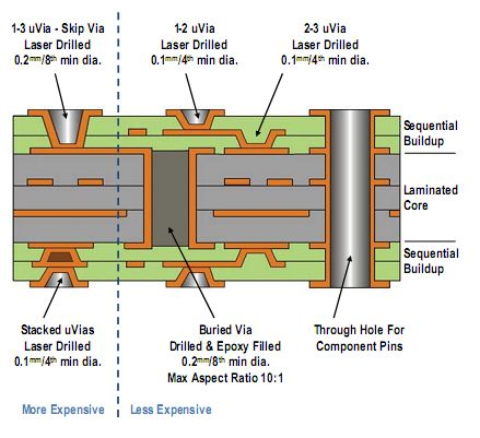
Conventional PCBs relied on mechanical drill bits for PTH drilling, as well as for blind or buried via drilling. However, with the advent of HDI circuits, the diameter of blind and buried vias went down to 100 um and below, and this was impossible to achieve using mechanical drill bits. For making the tiny holes, namely microvias, manufacturers had to resort to laser drilling.


Today, HDI PCB manufacturers use CO2 lasers in conjunction with high precision, high-speed scanner systems. A laser beam requires focusing and works by ablating the material on which it is focused. Therefore, it is only possible to make holes of limited depth using lasers. However, this suits the HDI boards, as manufacturers use lasers only to make blind or buried vias.


The HDI board manufacturing process uses copper direct drilling with a laser beam for creating bling or buried vias. In the process, a laser drills a blind via by first penetrating the surface foil, where the energy of the laser transfers to the copper foil and evaporates it. Then the laser burns through the substrate layer and stops on the surface of the inner copper layer. This is a high-speed process, and a 2-head CO2 laser-drilling machine can drill 1500-3000 holes per second for the copper direct processing of an HDI board.


For blind microvias with diameters of 40 um, although manufacturers use UV lasers, newer type of CO2 lasers are available. The latter are more economically efficient than UV lasers, as the machine splits the CO2 laser into four parts, uses special high-performance lens for each beam, and processes four holes at a time. Such machines are capable of drilling more than 4500 holes per second.


Creating double-sided PTH vias in boards with copper layers on both the top and bottom sides requires a different approach. The fabricator starts by using a laser beam to drill a hole half-way to the board thickness, then turns the board over and drills a hole from the other side at the same position—thus creating one through-hole. As the laser drilling position accuracy is less than ±10 um, double-sided drilling of through-holes of less than 100 um diameter does not cause displacements. Manufacturers are adopting the laser PTH drilling technique rapidly as it offers several advantages over conventional mechanical drilling, such as better hole positioning accuracy, high productivity, and offsetting drill-bit costs.


Advantages of Laser Drilling for Vias and Microvias


The major advantage in using laser drilling for vias and microvias is the hole diameter can be 50 um or less. As the vias take up less real estate on the board, the designer has more space for achieving higher wiring density. This has the effect of making an HDI board smaller and/or reduces the number of layers, thereby reducing the overall cost of the board.


Another advantage is the high-peak-power CO2 laser pulse can process the surface copper foil cleanly. It produces fine-quality blind vias holes that have smooth wall surfaces. This helps the plating process fabricators perform after the laser drilling, thereby strengthening the integrity of the plating process, and the quality and durability of the HDI PCB overall.


Conventionally, PTH drilling takes up a lot of real estate on the board. Rather than use PTH drilling, fabricators prefer a combination of blind and buried vias and microvias, as they can be stacked on above the other to achieve the same functionality as a double sided PTH. The designer has the flexibility either to stack up the vias and microvias or to stagger them to achieve higher wiring density. Designers often use landless microvias and via-in-trace technology for achieving even higher wiring densities.


Apart from using vias and microvias for conducting signal and power from one circuit layer to another, designers also use them for conducting heat away from a component generating heat while in operation. However, this requires filling the vias with copper or other heat-conducting material.


Conclusion


Successfully manufacturing HDI circuits with blind or buried vias and microvias requires special equipment and processes such as sequential lamination cycles, laser direct imaging, plugging, and laser drills. Moreover, as HDI boards use thinner layers, tighter annular rings and spacing, along with thinner specialty materials, manufacturers require additional time and significant investments in manufacturing equipment and processes.


About the Author 


Akber Roy is the CEO of RUSH PCB Inc. Akber Roy has 20 years of experience of electronic contract manufacturing. RUSHPCB Inc provides detailed printed-circuit-board development resources.

linked in icon
Sign up for HardwareBee
* = required field

Recent Stories

CEO Talk: Maarten Kuper, QBayLogic
Low ESR Capacitor: Ultimate Guide
The Ultimate Guide to PWM Controller
What is a Piezo Driver IC and how to Choose one
Introduction to Hall Effect Sensor ICs
The Ultimate Guide to: Oscillator ICs
Low Noise Amplifier: Ultimate Guide
ASIC Prototyping
Get 3 Quotes from Electronic Design Companies
Get 3 Quotes from FPGA Design Companies
Get 3 Quotes from Embedded SW Services
Get 3 Quotes from EMS Companies

Find Design Services

Get IC Prices

Get Price Offers From
  • Electronic Design Services
  • FPGA Design Services
  • Embedded Software Companies
  • PCB Layout Services
  • Printed Circuit Board Manufacturers
  • Design & Manufacturing Services
Welcome New Vendors
  • VVDN Technologies
  • Spark Product Innovation
  • QBayLogic
  • Fidus Systems
  • nao.design
Browse Vendor Directories
  • Electronic Design Companies
  • FPGA Design Companies
  • Embedded Software Services
  • Manufacturing Companies
Featured Vendor

DAB-Embedded

Recent Posts
  • CEO Talk: Maarten Kuper, QBayLogic
  • Low ESR Capacitor: Ultimate Guide
  • The Ultimate Guide to PWM Controller
  • What is a Piezo Driver IC and how to Choose one
  • Introduction to Hall Effect Sensor ICs
Most Popular Blog Posts
  • FPGA for AI (Artificial Intelligence): Ultimate Guide
  • PCB Stackup: Ultimate Guide and Examples
  • FPGA Video Processing: Ultimate Guide
  • The Ultimate Guide to Logic Chips
  • Cost of Electronic Manufacturing: A Guide

Never miss an update!

Follow us on LinkedIn

Do you need any price
information?

(Electronic design, FPGA design, Embedded SW services, PCB design, Turnkey)

Yes
No
This page is sponsored by
HardwareBee

Copyright 2017-2024, HardwareBee. All rights reserved.

  • About Us
  • Contact
  • Subscribe
  • News
  • Get Free Support
  • Get listed
  • Send a wiki/article
  • Advertise

Follow Us

Be sure to follow our LinkedIn company page where we share our latest updates LinkedIn
Partner with us Partner with us

Design and Manufacturing Services

  • Engineering Design Services
  • Electronic Design and Manufacturing
  • Electronic Product Development
  • Electronic Product Design
  • Electronic Consulting Services
  • Electronic Engineering Companies
  • Electronic Engineering Services
  • Electronic Product Design and Development
  • Electronics Design Services
  • Electronics Design Company
  • Electronic Design Consultants
  • Electronic Design Company
  • FPGA Design Company
  • FPGA Consultant
  • FPGA Design Services UK
  • Electronics Manufacturing services
  • Electronics Manufacturing Companies
  • Electronic Contract Manufacturing Companies
  • Electronic Manufacturing Services Companies
  • EMS Companies Directory
  • Electronic Design Services
  • FPGA Design Services
  • Embedded Software Companies
  • PCB Layout Services
  • Printed Circuit Board Manufacturers
  • Design and Manufacturing Services
X

Don’t miss anything, follow us on LinkedIn

https://www.linkedin.com/company/hardwarebee/

We are using cookies to give you the best experience on our website.

You can find out more about which cookies we are using or switch them off in .

Privacy Overview

This website uses cookies so that we can provide you with the best user experience possible. Cookie information is stored in your browser and performs functions such as recognising you when you return to our website and helping our team to understand which sections of the website you find most interesting and useful.

Strictly Necessary Cookies

Strictly Necessary Cookie should be enabled at all times so that we can save your preferences for cookie settings.

If you disable this cookie, we will not be able to save your preferences. This means that every time you visit this website you will need to enable or disable cookies again.

3rd Party Cookies

This website uses Google Analytics to collect anonymous information such as the number of visitors to the site, and the most popular pages.

Keeping this cookie enabled helps us to improve our website.

Please enable Strictly Necessary Cookies first so that we can save your preferences!

Additional Cookies

This website uses the following additional cookies:

(List the cookies that you are using on the website here.)

Please enable Strictly Necessary Cookies first so that we can save your preferences!