Successive Approximation Analog To Digital Conversion (ADC) Explained
23/02/2023, hardwarebee
Successive Approximation is one of the most widely used methods of digitizing an analog signal. The majority of successive approximation ADCs have an n-bit resolution and a maximum sampling rate of 5 MBPS.
Successive Approximation DAC has more complex circuitry than digital ramp ADC but results in faster conversions. This method is quite popular; it uses the binary search algorithm for the conversion process. It generates a sequence of approximations through all possible quantization levels. It assumes a trial digital number. It then converts the assumed digital number back into analog form (an internal DAC is there to convert a digital signal to an analog signal, VDAC). The comparator then compares the resulting analog signal VDAC with the input signal Vin.
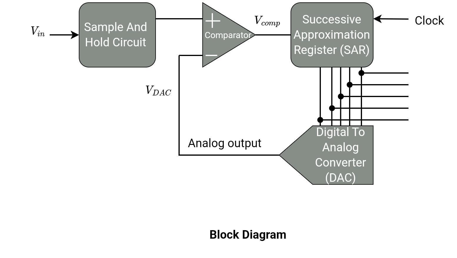
The block diagram below consists of 4 major blocks:
- A comparator
- A successive approximation register (SAR)
- A Digital analog converter (DAC)
- Sample and hold circuit (S/H)
Basic Building Blocks
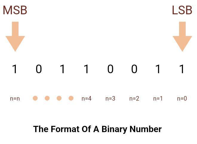
An analog signal is the input of an analog-to-digital converter (obviously). And the output is a digital signal. An analog signal is a continuous signal with infinite values. Whereas digital signals are not continuous and discrete. They have some finite levels, usually two or more levels. In most cases, digital signals are in binary format. It has either low or high levels (either 1 or 0).
Sample And Hold Circuit
The first block in the block diagram is the sample-and-hold circuit. It creates samples of an input signal and holds these samples at a constant level for a definite period of time. The value remains unchanged until the next sample arrives. They are particularly used in ADC to produce a discrete signal. Modern ADC chips frequently have a sample and hold circuit of their own. This discrete signal will then appear at the comparator input.
Comparator
A comparator is an electronic circuit that compares two analog signals. In this ADC, the first input is the input signal, and the second signal is the output from the DAC. The comparator determines whether the feedback voltage is larger than the input signal, and depending as before on the result of the comparison, this bit is either allowed to remain or is cleared.
In each clock cycle, the comparator compares the two signals. The comparator compares Vin with VDAC.
Vin Versus VDAC
Vin > VDAC: Comparator output goes low. The bit in the SAR goes low as well.
Vin < VDAC: Comparator output goes high. The SAR keeps that bit high.
The output of the comparator is connected to the SAR. In this way, the DAC output voltage approaches the input voltage gradually. The comparator differential output also approaches zero.
Successive Approximation Register SAR
It is a register that contains a digital representation of the analog voltage stored in the SAR. On the first clock cycle after receiving the conversion instruction, it starts with all zeros in SAR.
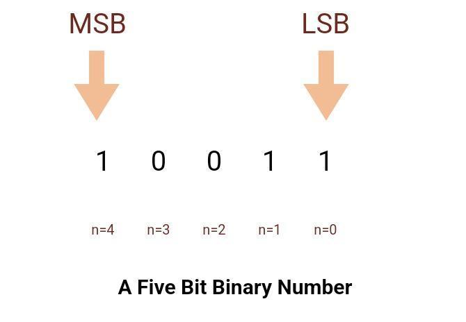
Let’s suppose an n-bit binary number. The approximation starts from the nth bit or MSB.
This register’s contents change bit by bit, beginning with MSB (the nth bit) and ending with LSB (n = 0).
Every clock cycle modifies the register’s content. The output of the SAR is fed to the DAC.
The conversion procedure is complete when the value of this register matches the analog input voltage.
Digital To Analog Converter DAC
An internal DAC is used to generate approximations of the input voltage. It produces an internal analog output voltage that is equivalent to the output of SAR (the output of the SAR is in digital format). This signal will appear at the negative terminal of the comparator, as shown in the block diagram.
Working Principle
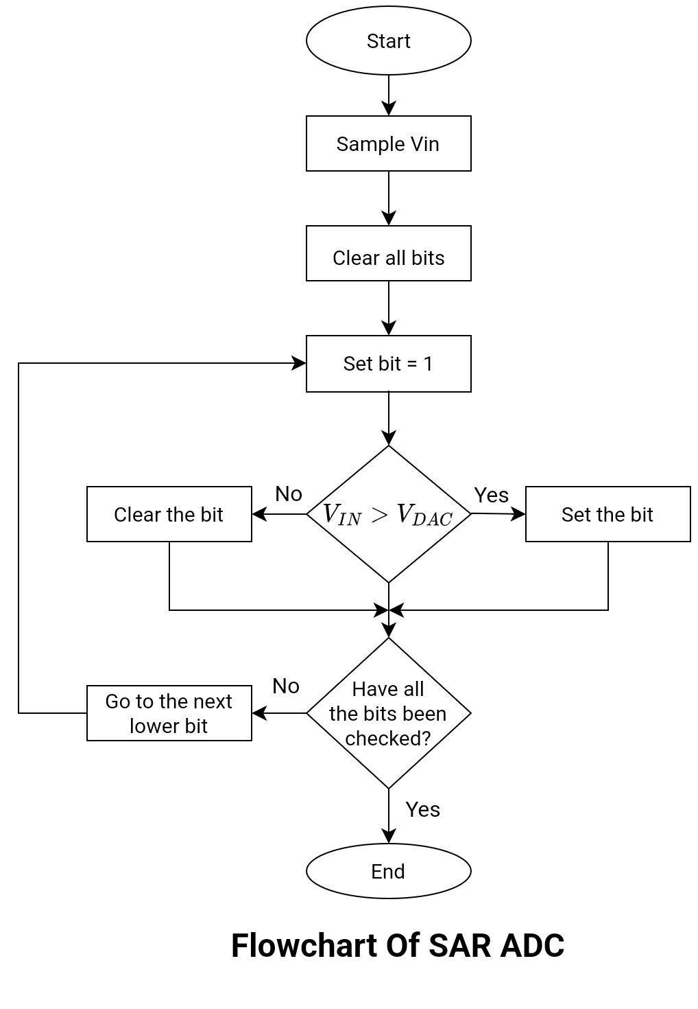
The basic working principle is better understood with the help of an example and a flowchart.
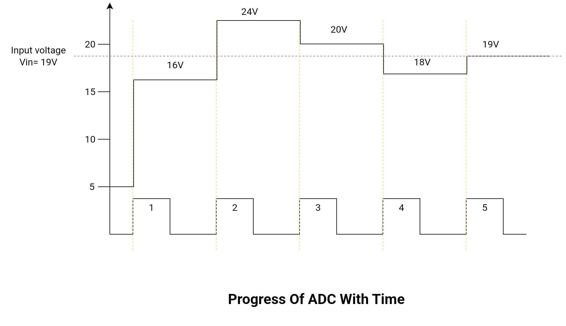
Suppose a five-bit SAR ADC. An analog voltage signal of 19 volts is applied at the input.
Vin = 19V
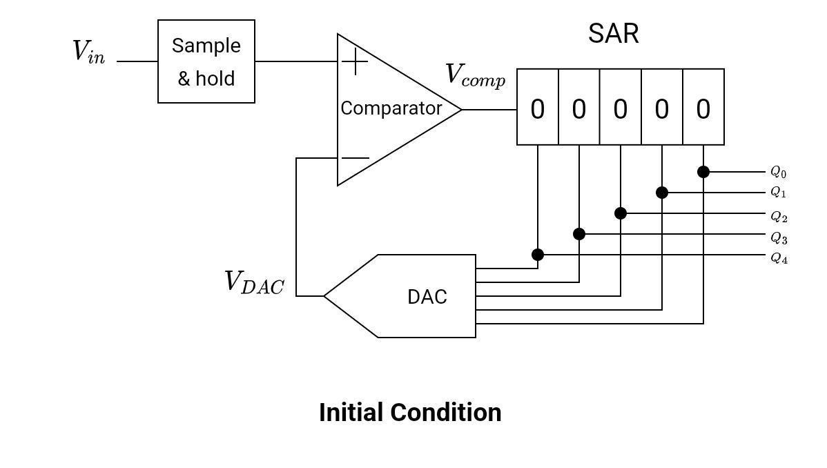
Initial Condition
The operation starts by clearing all the bits in SAR. Let’s suppose Q is the output, since it is a 5-bit ADC, the output will have five bits from Q0 to Q4. Initially, the contents in successive approximation register (SAR) are given below:
Q = [00000]
VDAC = 0V
Vin > VDAC
Vcomp = high
First Clock Cycle
The comparator output is connected to SAR. As the comparator output goes high, the device sets the SAR’s most significant bit to one while leaving the other bits at zero.
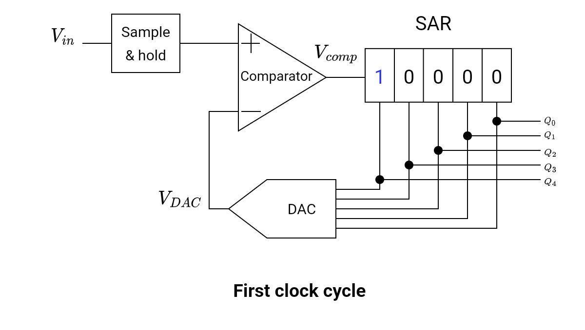
The outputs of the circuits during this clock cycle are given below.
Q = [10000]
VDAC = 16V
Vin < VDAC
Vcomp = low
Keep in mind that the output from DAC is the equivalent of the contents in SAR. The figure below shows the contents of the SAR register during the first clock cycle.
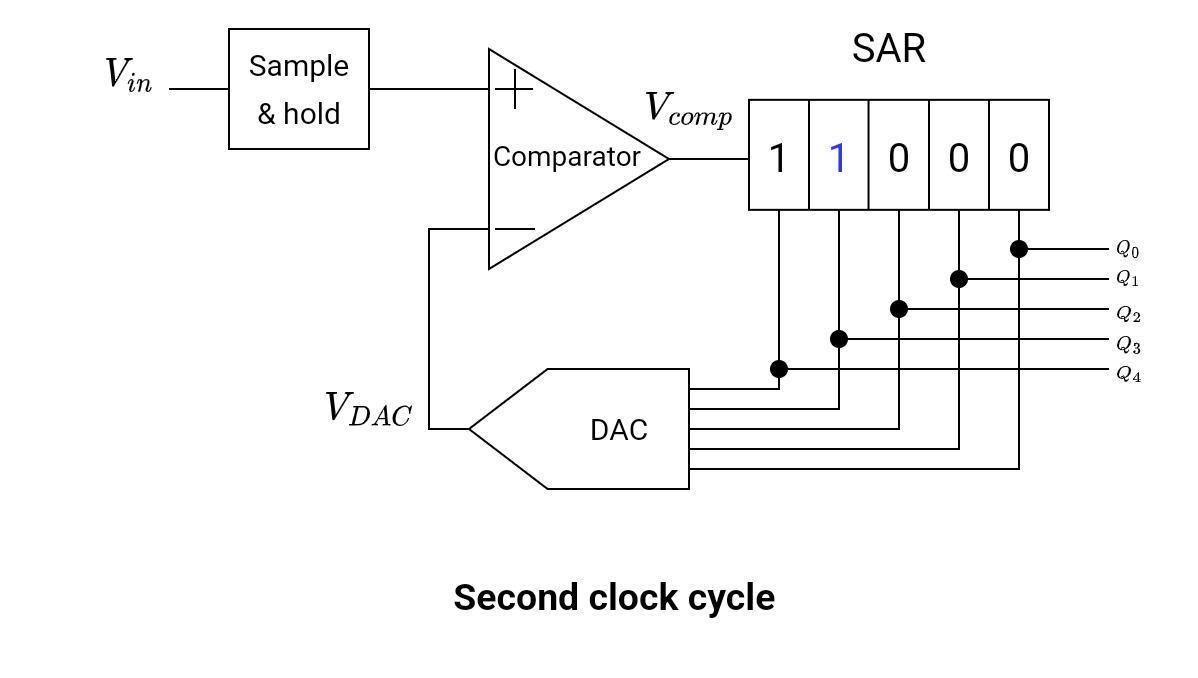
Second Clock Cycle
Again, the same procedure will be followed. This time the n-1 bit (that is, the 4th bit) is set to 1, while all other bits remain unchanged.
Q = [11000]
VDAC = 24V
Vin < VDAC
Vcomp = low
The figure below shows the contents of the SAR register during the second clock cycle.
And
In this clock cycle, the output of the comparator goes low. The n-1 bit is set to a low value.
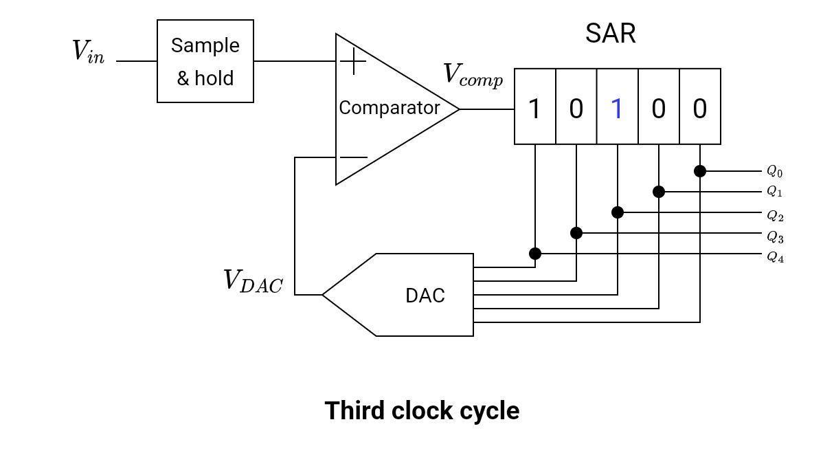
Third Clock Cycle
In this clock cycle, the n-2 bit (that is, the 3rd bit) is set. while the value of the previous n-1 bit is 0. The value of SAR in the second clock cycle was Q = [11000] = 24V.
The value of the SAR register during the third clock cycle is given below.
Q = [10100]
VDAC = 20V
Vin < VDAC
Vcomp = low
The figure below shows the contents of the SAR register during the third clock cycle.
But this value (Q = 10100 or VDAC = 20) is greater than the input voltage.
The approximation is wrong. The output of the comparator goes low.
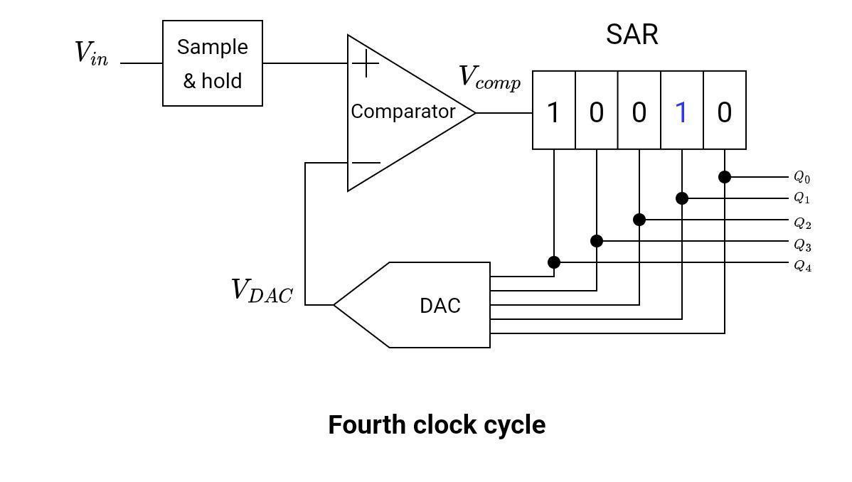
Fourth Clock Cycle
In this clock cycle, the n-3 bit (the second bit) is set. while the value of the previous n-2 bit is 0. The value of SAR in the third clock cycle was Q = [10100] = 20 V. But this value is greater than the input voltage. Again,n the approximation is wrong. The n-2 bit goes low while the n-3 bit goes high.
Q = [10010]
VDAC = 18V
Vin < VDAC
Vcomp = high
The figure below shows the contents of the SAR register during the fourth clock cycle.
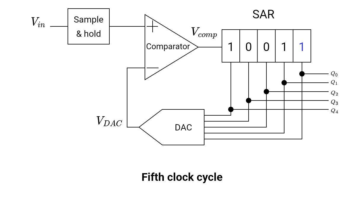
Fifth Clock Cycle
In this clock cycle, the n-4 or LSB bit is set. while the other bits remain unchanged. The value of SAR in the fourth clock cycle was Q = [10010] = 18V. But this value is less than the input voltage. The comparator output goes high. The least significant bit goes high.
Q = [10011]
VDAC = 19V
End of conversion
The figure below shows the contents of the SAR register during the fifth clock cycle.
At the end of the conversion, the input of the DAC is equal to the output of the DAC.
Successive Approximation ADC Specifications
There are several important parameters for determining the precision of an ADC:
- Sampling rate
- Quantization error
- Resolution
- Conversion time
- Aliasing effect
Sampling Rate
The sampling rate of the ADC should be at least double the frequency of the input signal.
It is suitable for applications where sampling is 10 MSPS.
Quantization Error
An analog signal is a continuous signal, whereas a digital signal is represented by discrete values (discrete in time and amplitude). Quantization error is the difference between an actual analog value and its digital reconstruction. As the number of bits increases, the quantization error reduces.
Resolution
The resolution of these types of ADCs is quite high. It ranges from 8 bits to 16 bits. An n-bit ADC has 2n different voltage levels. For example, a 4-bit ADC has 16 different voltage levels. So, as the number of ADC bits increases, resolution increases. Higher resolution results in improved signal quality.
Conversion Time
It is the time taken by an ADC to completely digitize an incoming analog signal. For higher-speed conversions, a lower conversion time is required.
In this type of analog-to-digital converter, the conversion time is independent of the input signal. The processing of one bit requires one clock cycle. For an n-bit converter, n-clock cycles are required. So, there is a general formula for conversion time.
TC= n*Tclock
Where,
TC = Conversion time
Tclock = Time taken by the clock signal
Aliasing Effect
As discussed above, the conversion time is given by:
TC= n*Tclock
There should be “nT” time required to complete a single conversion. The next input sample should be taken after nT clock pulses.
Advantages
- High Accuracy: Successive approximation ADCs offer high accuracy compared to other types of ADCs, making them suitable for applications that require precise measurements.
- Speed: They are faster than other types of ADCs, as the conversion process takes only a few clock cycles. This makes them suitable for high-speed applications.
- Low power consumption: Successive approximation ADCs consume less power than other types of ADCs, making them ideal for battery-powered devices.
- Simple Circuitry: The circuitry of a successive approximation ADC is relatively simple, requiring fewer components than other types of ADCs.
- Easy to Interface: They are easy to interface with microcontrollers or digital signal processors (DSPs), making them suitable for use in digital systems.
- Noise immunity: Successive approximation ADCs are less susceptible to noise and interference, resulting in a more accurate output.
- Flexible Resolution: The resolution of a successive approximation ADC can be easily adjusted by changing the number of clock cycles, making it versatile for different applications.
Disadvantages
- Slow Conversion Rate: The successive approximation ADC requires a certain amount of time to complete each conversion. This process is slower than other types of ADCs, such as flash ADCs, which can produce results almost instantly.
- Limited Resolution: The resolution of a successive approximation ADC is limited by the number of bits in the digital-to-analog converter (DAC). This means that the accuracy of the conversion can be compromised if the resolution is not high enough.
- Non-linear Behavior: The successive approximation ADC may exhibit non-linear behavior when converting analog signals. This can result in errors in the conversion process, which can affect the accuracy of the final output.
- Susceptibility to Noise: The successive approximation ADC is more susceptible to noise than other types of ADCs. This can lead to errors in the conversion process and affect the accuracy of the output.
- Complexity: The successive approximation ADC is more complex than other types of ADCs. This can make it more difficult to design and implement, and can also increase the cost of the system.
Applications
Successive approximation ADCs are commonly used in applications where precision and accuracy are critical, such as in medical equipment, scientific instruments, and industrial automation systems. Some specific applications of successive approximation ADCs include:
- Data acquisition systems: These ADCs are used in applications where precise measurement and digitization of analog signals are required, such as in temperature, pressure, and vibration sensors.
- Digital audio recording and playback: Successive approximation ADCs are used in audio recording and playback equipment, where high-resolution audio signals must be digitized and stored in digital formats.
- Medical equipment: Successive approximation ADCs are used in medical equipment such as electrocardiograms (ECGs), blood pressure monitors, and other diagnostic tools where high accuracy is required.
- Industrial automation: Successive approximation ADCs are used in industrial automation systems such as motion control, robotics, and process control, where precise measurement and control of analog signals are necessary.
- Communications: Successive approximation ADCs are used in communication systems such as modems and digital signal processing equipment, where analog signals must be digitized and processed for transmission or storage.