Understanding Tunnel Diode
02/02/2023, hardwarebee
Introduction
General diodes can block the current in one direction and allow the current to flow in the opposite direction, which can be used for providing DC parameters. However, other types of diodes are available that can be employed for various purposes. In this article, one of the diode types, namely, tunnel diode, is discussed in detail. To cover all the grounds about this specific diode, the tunnel diode history is explained first, together with its symbol in electric circuits. Then, the tunnel diode basics and structure are introduced to provide more detailed information about the tunnel diode features. Finally, its applications and band diagram are presented to summarize the article.
Tunnel Diode Basics and History
Like general diodes, tunnel diode has two terminals including anode and cathode because it is also made of a narrow P-N junction (100 nm wide). However, its symbol in electric circuits is quite different. Figure 1 illustrates the tunnel diode symbol, which has two terminals. Tunnel diode also called Esaki diode since it was invented by Leo Esaki in 1957. In fact, Esaki worked on quantum mechanical effect with Yuriko Kurose, and Takashi Suzuki at Sony, and based on that, he won the Nobel Prize in Physics for discovering electron tunneling effect, which had been used for tunnel diode structure. This type of diode first manufactured by Sony at that year, and from 1960 onwards, other companies like General Electric (GE) have started manufacturing of tunnel diode. In quantum mechanical tunneling phenomenon, a free electron can pass through a potential barrier while the depletion region is very thin. Due to high-speed switching characteristic of tunnel diode, it is utilized in microwave applications. Applications of this diode will be discussed further in the following section.
Figure 1: Tunnel diode symbol in electric circuits with two terminals, including Anode and Cathode
Tunnel Diode Structure
As mentioned before, a tunnel diode is basically a P-N junction, which has some specific features. This junction is a boundary between two p-type semiconductors and an n-type one. In an n-type semiconductor, electrons predominate, but in a p-type semiconductor, holes outnumber electrons. In this case, electrons can pass the P-N junction in one direction in general diodes. Therefore, diodes can be used for rectification. Although tunnel diode has P-N junction similar to general diodes, its behavior is a bit different from them, which can be used for some specific applications. The first difference is that the doping concentration of the p-type layer and n-type layer in the tunnel diode is extremely high. Another thing is that the p-type layer is much smaller than the n-type layer in the tunnel diode. In terms of material, gallium arsenide, gallium antimonide, and silicon can be used in tunnel diode fabrication. Since the p-type and n-type layers are highly concentrated, the depletion region is considerably narrow. The tunnel diode structure and P-N junction in this type of diode are presented in Figure 2.
Figure 2: Tunnel diode structure and P-N junction
Tunnel Diode Characteristics
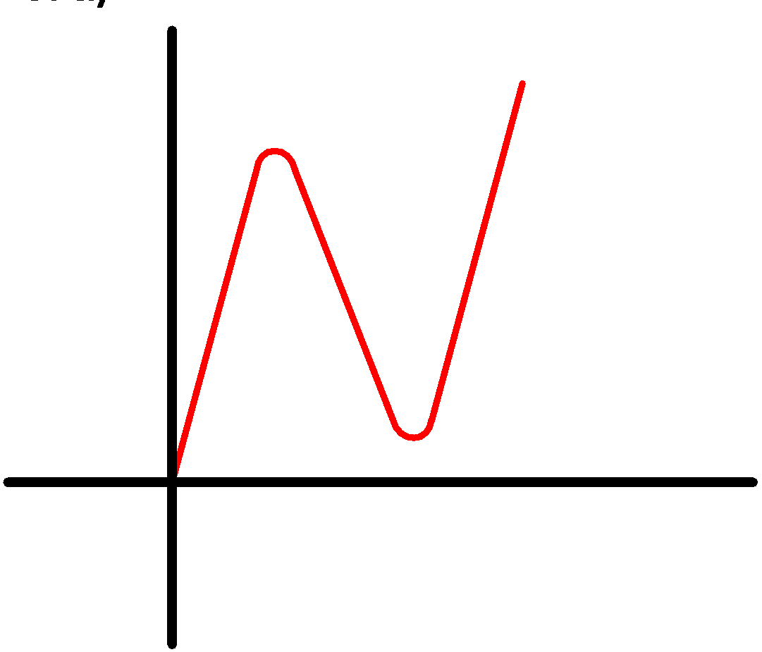
In this type of diode, the V-I characteristic is completely different from the typical diodes. In general diodes, when the anode voltage is higher than the cathode voltage, by considering the voltage drop of the diode, the diode will be in forward bias, and the current goes up while the voltage increases. However, there is a special behavior in tunnel diodes. Similar to the general diodes, when the voltage increases across the tunnel diode, the current also rises to a certain amount (peak point). Passing the peak point, the current goes down by increasing the voltage, which means that there is a negative resistance region in the tunnel diode. In this region, the current decreases to reach a minimum value called valley point. After the valley point, the current rises again by increasing voltage like general diodes. The tunnel diode characteristic is shown in Figure 3.
Figure 3: Tunnel diode V-I characteristics with peak and valley points
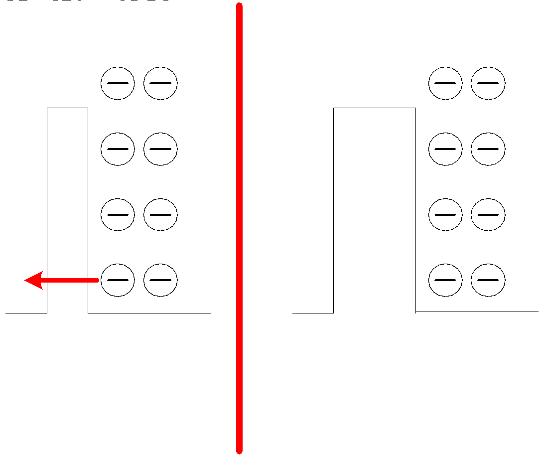
To understand this characteristic, the P-N junction must be studied in detail. The difference between the P-N junction in the general diode and the tunnel diode is the junction width. As the layers are highly concentrated in tunnel diodes, the junction width is relatively narrow, while the junction width in general diodes is quite wide. Figure 4 depicts the junction width in tunnel diodes and general ones. In a normal diode, the electrons with high energy can pass the barrier to jump to the p-type layer when the diode is in forward bias. In this case, the electrons with lower energy are not able to pass the depletion region because the junction width is quite high. However, the tunneling effect can happen in a tunnel diode because the depletion region is relatively narrow. Therefore, in forward bias, electrons with higher energy move to the p-type layer when the voltage goes up from zero to the peak point. After the peak point, electrons with lower energy can also pass the junction by penetrating through the depletion region. This phenomenon can be explained by the quantum mechanical effect. For a better understanding, the energy band diagram is presented in the following section.
Figure 4: P-N junction in a general diode and a tunnel diode
Tunnel Diode Energy Band Diagram
At first glance, tunnel diode behavior is quite complex, but the energy band diagram can help us to understand what happens inside the tunnel diode and why a negative resistance region is created in this type of diode. The tunnel diode is studied in four different points to cover all conditions. This phenomenon is due to a narrow P-N junction and highly concentrated layers (thousands of times greater than general diodes). In no bias condition, the voltage and current are zero. The reason is that when the voltage is zero, there is no energy for electrons to pass the gap and reach the holes, and no current will flow through the tunnel diode. In the tunnel diode, there are bands, including the conduction band and valence band. Due to heavy doping in the tunnel diode, there is a level, namely, the fermi level, which is in the conduction band inside the n-type layer, and inside the valence band in the p-type layer. As can be seen in Figure 5, the fermi levels in both layers are the same because zero voltage has been applied to the tunnel diode.
Figure 5: Tunnel diode energy band diagram in zero voltage
When a forward voltage is applied to the tunnel diode, the Ef level in the n-type layer goes higher, and the difference between levels will be equal to the applied voltage. In this case, there is an overlap between electron and hole regions, as shown in Figure 6.
Figure 6: Tunnel diode energy band diagram when voltage goes up from zero
Since the junction width in the tunnel diode is extremely narrow, and there is an energy state on the other side, the electrons in the n-type layer can move to the p-type layer and fill the holes through a tunnel. It means that the electrons can go through the tunnel instead of surmounting the barrier, and the current flows through the tunnel diode. Increasing the applied voltage will increase the overlap, and the current will rise because more electrons can traverse through the tunnel to the p-type layer. The peak point is the point that the hole, and electron regions are equal. Passing this point, the overlap region decreases again because the Ef level in the n-type layer goes higher, meaning that the current in the tunnel diode declines, as shown in Figure 7.
Figure 7: Tunnel diode when voltage pass the peak point
Higher voltage lower overlap region and current. Thus, the current goes down to reach around zero, which is the valley point. After the valley point, the tunnel diode is similar to a general diode, and electrons must surmount the barrier without tunneling. In this case, the current increases again by increasing the applied voltage, as shown in Figure 8.
Figure 8: Tunnel diode energy band diagram after valley point
In the reverse bias, the story is different because the applied voltage increases the distance between regions. Unlike general diodes, the current is zero in reverse bias, the minor electrons in the p-type layer can tunnel through the junction, and there is empty space in the n-type layer. Therefore, the negative current will flow through the tunnel diode, and the V-I curve in reverse bias is linear, as depicted in Figure 9.
Figure 9: Tunnel diode energy band diagram in reverse bias
Advantages, disadvantages, and applications of tunnel diode
Like other types of diodes, tunnel diode also has some benefits and drawbacks, which makes them special for some purposes. The advantages of tunnel diodes are long life, high-speed operation, low noise, and low power consumption. In terms of disadvantages, it can be noted that the tunnel diodes cannot be fabricated in large numbers, and input and output terminals are not isolated from one another. Tunnel diodes can use for different purposes, i.e., they can be used as logic memory storage devices, relaxation oscillator circuits, ultra high-speed switches, and FM receivers.


