
Understanding DV/DT in Electronics
14/11/2022, hardwarebee
High-speed switching circuits, like SCR, MOSFETs, and BJTs, are sensitive to the rate of change (rise) of the voltage applied to the device. In switching circuits, dV/dt represents the instantaneous rate of change of voltage with respect to time (volts per second increase or decrease).
The dV/dt rating of any semiconductor device is an important parameter since it demonstrates the maximum rate of rise of applied voltage that does not bring the device into conduction or false turn-on. It must be less than the specified dV/dt limit of the device.
Turn-off snubber circuits are employed to overcome this problem. They help to prevent the sudden rise of dV/dt across the device. These circuits are not only used in the suppression of high-voltage transients but also offer many benefits:
- Reduce switching losses and transfer them to an external resistor.
- Reduce noise and EMI
- Prevent the second breakdown in BJT switches
DV/DT in BJT
In BJT switching circuits, it is the rate of rise of the collector to emitter voltage.
In these switching circuits, there are some delays associated with switching speed like delay time and storage time. Ignoring these two delays, BJT switching waveforms are like this.
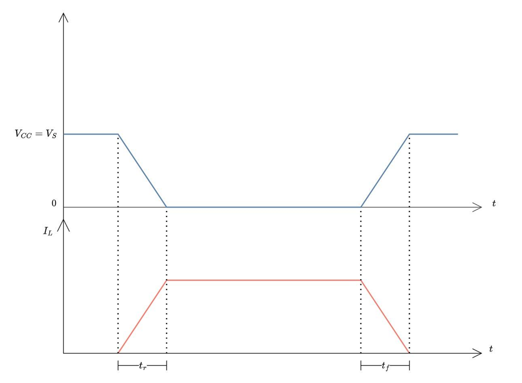
Figure 1: BJT switching waveforms
During turn-off time, dV/dt should be within limits. For a power BJT collector current, IC falls, and VCE should not rise immediately. Otherwise, a second breakdown may occur. To control the rate of rise of VCE, a simple RC snubber circuit is connected in parallel with BJT or in between collector and emitter junctions. It limits the rate of a sudden rise in VCE during turn-off time.
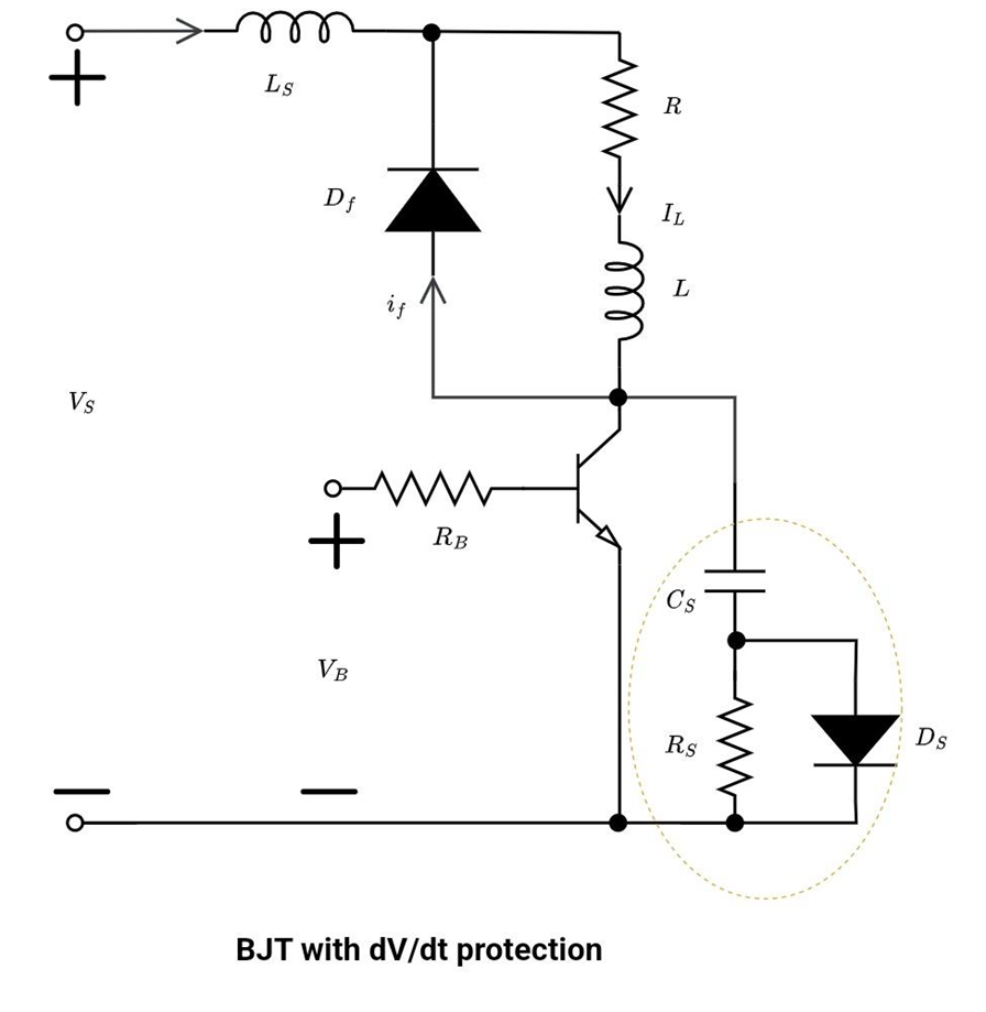
Figure 2: A BJT transistor with dV/dt protection
Have a look at the circuit diagram. DS, CS, and RS constitute a snubber circuit. During turn-off time, the equivalent circuit is given below.
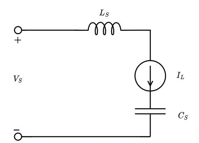
Figure 3: Equivalent circuit during turn-off time
As the BJT turns off, the DS turns on.
The capacitor CS is charged by the load current IL (assume IL is freewheeling through diode Df). The load current flows through the capacitor and charges it linearly up to VS. Once the capacitor is charged, the resistor RS is there to provide the discharging path.
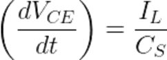
The above equation shows the dV/dt across the transistor during off time. By choosing suitable values of CS and RS, it is possible to limit the dV/dt across the transistor.
DV/DT in MOSFETS
In MOSFETs, it is used to specify the switching transient period. In other words, it is the rate of change of voltage Vds (drain-source voltage) caused by switching influence. Power MOSFETs are designed for switching purposes. When it operates in a linear region, it has large transconductance, parasitic capacitance, and stray inductances (between gate and source and other interconnections) that probably form a positive feedback path and stimulate undesirable or parasitic oscillations. This happens particularly during transient switching periods because of higher transconductance values. Interaction of high dV/dt with the circuit parasitic inductances and capacitances will result in overshoot and oscillations during the turn-off time. Due to these oscillations, the transistor is off and on repeatedly. It will result in high power dissipation, which may lead to burnout.
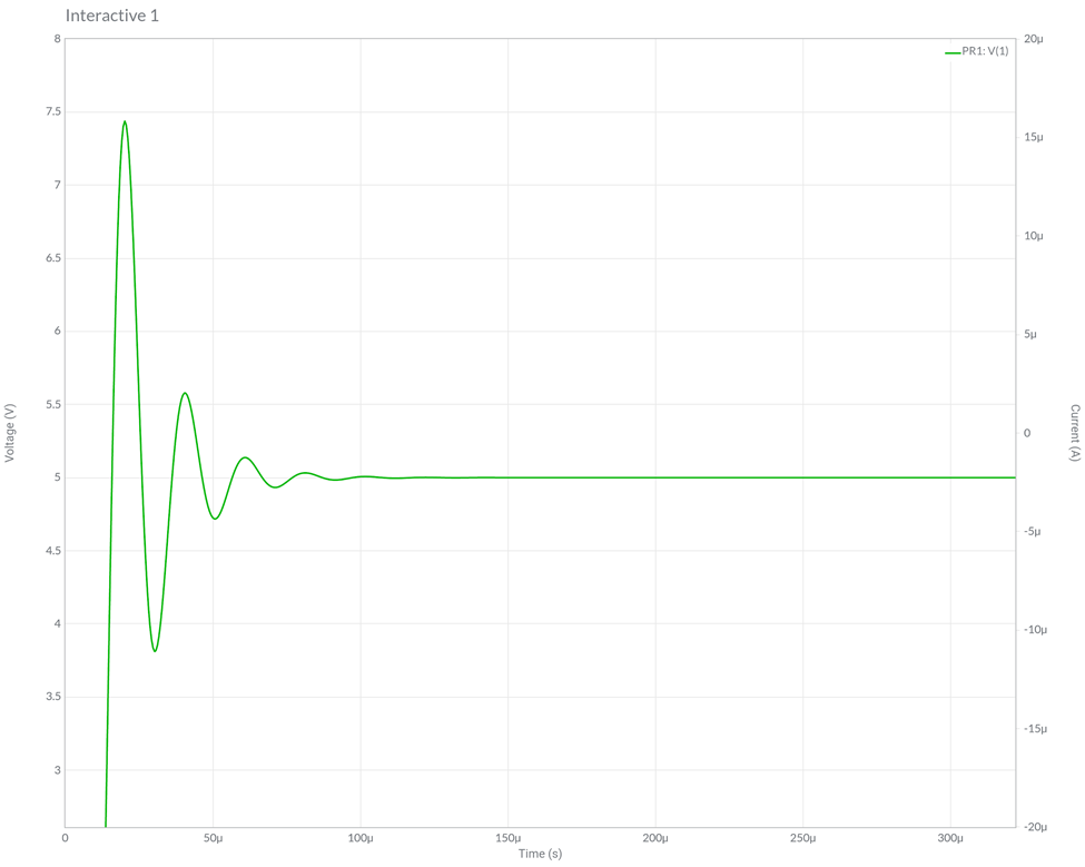
Figure 4: Ringing and overshoot
Two key ways can cause this dV/dt-induced failure.
The first effect is associated with parasitic BJT. If the applied voltage rises suddenly, it might turn on the MOSFET unintentionally when it is supposed to be off. There is a high voltage at the drain terminal, which may cause damage as well.
Let’s take a deep dive into this mechanism.
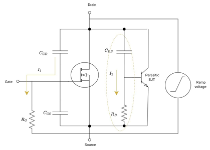
Figure 5: The parasitic BJT
- Consider the MOSFET in the off-state.
- Look at the capacitance CBD which is connected between the base of the NPN and the drain of the MOSFET. A rapid increase in voltage between the source and drain will generate a current I2.
- I2 will flow from RB. If the voltage drop across RB becomes greater than VBE then it will turn on parasitic BJT. It will drive the MOSFET into an avalanche, a destructive condition.
The dV/dt capability of this mechanism is given by:
![]()
There are several ways to avoid dV/dt:
- Reduce RB. It is a device parameter and a circuit designer can not control it.
- VBE and RB are temperature-dependent.
- It is better to control the switching speed of a MOSFET.
The second effect is active through the feedback action of internal capacitance between the gate and drain CGD.
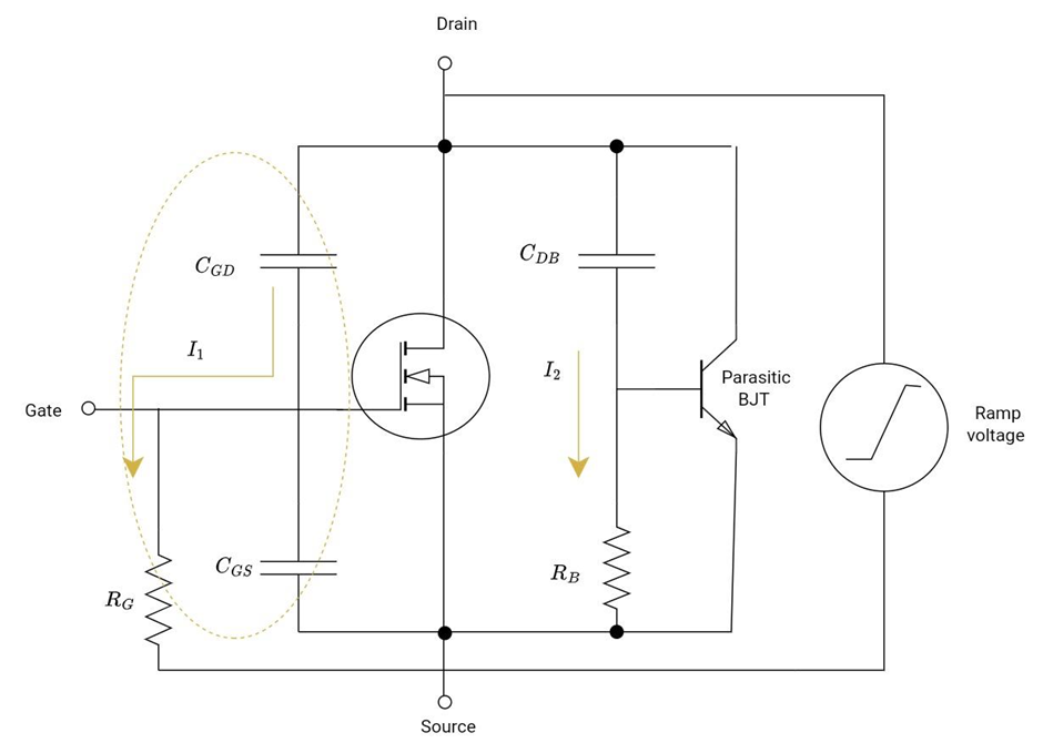
Figure 6: The feedback path because internal gate and drain capacitance
- Assume the transistor is off.
- Apply ramp voltage across the drain and source terminal. A sudden increase in the voltage Vds will result in current I1 due to CGD
- I1 will flow from RG. RG is the gate resistance and II is the current flowing through it. Then voltage across the gate terminal is given by:
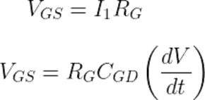
- If VGS becomes greater than the threshold voltage of the MOSFET (Vth), it will start conduction unintentionally. The dV/dt capability for this mechanism is given by:

There are several ways to avoid this condition:
- It is clear from the equation that low Vth devices are more likely to suffer from dV/DT.
- Vth is temperature-dependent.
- The Gate circuit is an important parameter, it is a device parameter. Higher gate oxide thickness reduces CGD and increases Vth. From the dV/dt relationship, decreased CGD will increase dV/dt capability.
DV/DT in Thyristors
In thyristors, dV/dt is the rate of change of applied anode to cathode voltage (VAK). It is also known as the rate of rise of OFF-state voltage. If dV/dt increases beyond the specific value stated in the datasheet, then it may cause a false triggering of SCR. The false triggering is caused by the internal junction capacitive current in the gate area. Let’s suppose the internal junction capacitance of the device is C. When the rate of rise of voltage across the anode to cathode (dVAK/dt) is very high, a displacement current ‘i’ is generated because of the internal capacitance. Even in the absence of external current flowing through the gate terminal, this current is sufficient to activate the thyristor. The system will unintentionally enter forward conduction mode as a result.
To avoid this condition, snubber circuits are used. The foremost objective is to prevent spurious turn-on of a thyristor due to the high rate of rise of the applied voltage (VAK). It is a series RC network. It is connected in parallel with the thyristor.
Let’s connect a single capacitor of a suitable value that is connected in parallel with a thyristor. When switch S1 is closed at t = 0, the voltage(VAK) is applied across the thyristor T. The dV/dt may be sufficient to turn on the device. The capacitor CS limits the rate of rise of applied voltage. The discharge current of the capacitor is limited by adding a resistor RS in series.
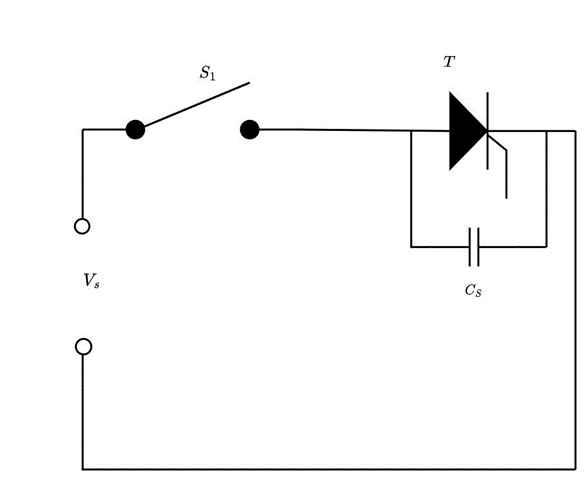
Figure 7: A snubber circuit without a discharging resistor.
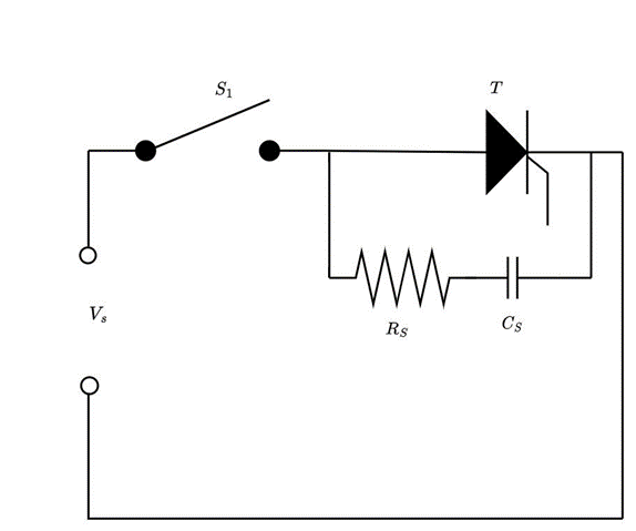
Figure 8: Illustration of a snubber circuit with a discharging resistor.
The voltage across the thyristor rises exponentially. It is limited by choosing suitable values of capacitor and resistor. The dV/dt can be determined with the help of the following formula:
![]()


