Understanding Knee Voltage
24/10/2022, hardwarebee
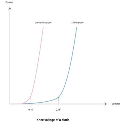
To understand the term knee voltage we should first refer to the graph of a diode (figure 1). The knee is the bent on the graph, after which rapid changes occur in the diode behavior. This bent is shaped like a knee, hence the term “knee voltage”.
This current-voltage graph (the VI characteristic curve of a diode) shows an unusual change in its conduction pattern. That change is an exponential growth of the current curve from almost non-conducting to an exponential rise of current through the device.
This is the knee voltage of the diode, and it is approximately equal to the barrier potential of the diode. It is a small forward voltage at which the current through the diode starts to increase exponentially. Therefore, this voltage is crucial for maintaining the right amount of current flowing through the diode.
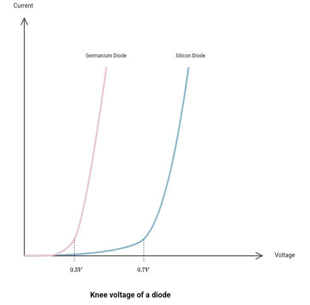
Figure 1: Knee Voltage of a Diode
Knee Voltage Background
Let’s delve into knee voltage from a theoretical perspective.
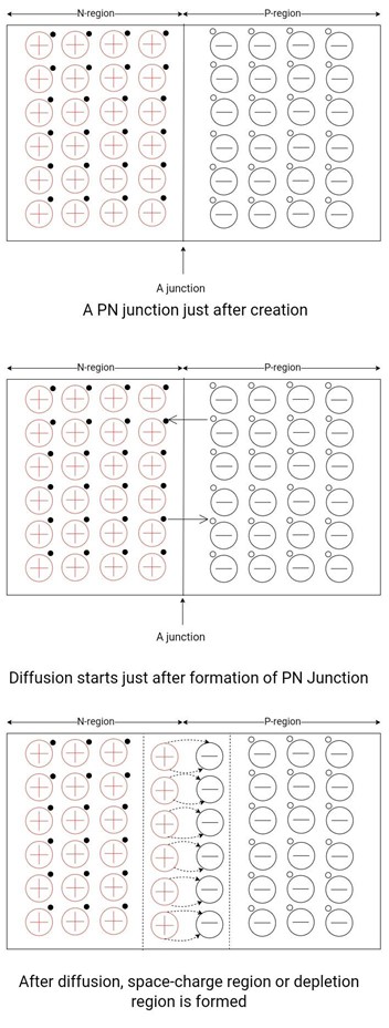
Let’s suppose no voltage is applied to the PN junction. It is a simple crystal, half of which is doped with p-type material (p-region) and the other half is doped with n-type material (n-region). Just after its formation, diffusion starts.
- The holes from the p-region diffuse into an n-region and combine with a free electron in the n-region. This creates an electron-hole pair (EHP).
- The electrons from the n-region diffuse into the p-region and fall into a hole in the p-type region. This creates an electron-hole pair (EHP).
Figure 2: Diffusion process and process of depletion region formation
There are only a few diffusions and recombination of electron-hole pairs. And this occurs at the junction of both regions only. This depleted region, or the space charge region, is responsible for the barrier potential. This region is automatically set up with a force that further prevents the diffusion of charged carriers (electrons and holes) from one part to another.
To make a diode forward biased, connect a voltage source across it. Initially, the diode current is negligibly small. As the applied voltage approaches the knee voltage, the width of the depletion region narrows and current increases rapidly. This is also known as the “cut-in voltage” or “threshold voltage.” For silicon diodes, it is 0.7V and for germanium diodes, it is 0.3V.
Figure 3: IV curves and knee voltages of silicon and germanium diodes
Knee Voltage in Schottky Diode
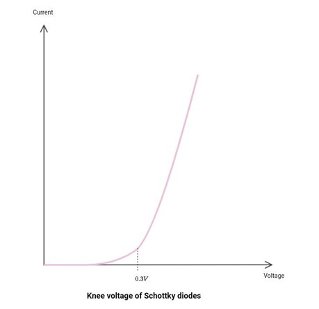
Unlike an ordinary silicon diode, Schottky diode construction is quite different. A moderately doped n-type semiconductor is joined with a metal junction to form a Schottky diode. So, there is a junction between metal and semiconductors. Under no bias condition, there is a tiny junction between the metal and the n-type semiconductor. When a voltage is applied, such that the positive terminal of the battery is connected to the metal junction and the negative terminal of the battery is connected to the n-type semiconductor, a small forward voltage drop is enough to overcome this barrier, and the current will start to flow rapidly. From the graph, it is observed that the knee voltage is 0.3V. The knee voltage and width of the metal-semiconductor junction may vary, as it greatly depends on the type of metal used in its construction.
Figure 3: Schottky diode characteristic curve (knee voltage)
Zener Diode Knee Voltage
The construction of a Zener diode is almost similar to an ordinary silicon diode but with heavy doping levels. This diode is used to work in reversed-biased mode, and it is known as the Zener breakdown. The Zener effect is achieved at a particular voltage, and this occurs at the knee voltage (Zener voltage).
Figure 5: IV Graph of Zener Diode
The Zener breakdown, or Zener effect, occurs through quantum tunneling. When a high reverse-biased voltage is applied at the PN junction, it will result in a sufficiently large electric field. This electric field is responsible for providing a force that pulls electrons away from their parent nuclei and becomes free carriers. This electrostatic force can tear the covalently bonded electrons, which causes a large amount of current. Due to this ionization, an electron-hole pair is created. Because of heavy doping, the depletion layer is very narrow, and the electric field intensity is quite intense for this narrow layer. As a result, breakdown occurs at lower voltages (about 6V).
Because of this heavy doping, a large number of EHP are created, and they constitute the large reverse current. To get this current, the minimum voltage required is known as the knee voltage or the Zener voltage. Zener breakdown usually occurs at 2*107 V/m. For a heavily doped diode, the knee voltage is 6V.
Light Emitting Diode Knee Voltage
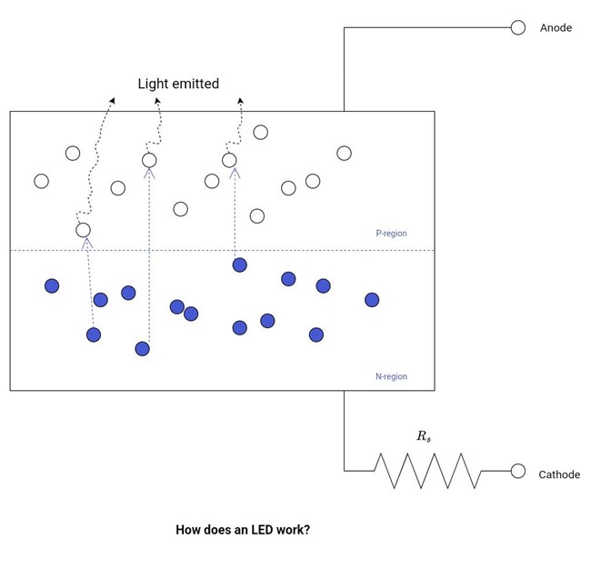
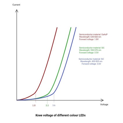
LED converts forward current into light. The construction and working principle of LEDs are similar to ordinary diodes. The only difference between them is the use of semiconductor material. Rectifier diodes are formed from silicon. LEDs are made up of semiconductor materials such as gallium arsenide phosphide (GaAsP) or gallium phosphide (GaP). These are the materials known for their direct bandgap. When a forward bias is applied, electrons from the conduction band recombine with vacant spaces or holes in p-type material. Due to this electron and hole recombination, excess energy is liberated in the form of radiation. The radiation has a specific colour and wavelength. The longer the wavelength of the emitted light, the lower the knee voltage. Different coloured LEDs use different materials. The materials producing shorter wavelengths require more energy to excite an electron to a higher valence band and hence a higher turn-on voltage.
Figure 6: Structure of an LED
When a forward-biased voltage is applied, there is a drop across the LED just like with ordinary diodes. This drop is equal to the threshold voltage or knee voltage. The knee voltage depends on the LED current, the color of the emitted light, and the semiconductor material used. At this point, the current starts to increase rapidly. In an LED, the rate of recombination of electron-hole pairs is directly proportional to the current. The higher the recombination, the higher the current. Also, the LED light intensity (or the output intensity) is directly proportional to the forward current.
Figure 6: Knee voltage of LED

