• Get Listed
    • Get a FREE Quote for your Next Project
HardwareBee
  • Find ASIC Vendors
  • Browse Design Services Directory
    • FPGA Design Services
    • Electronic Design Services
    • Embedded Software Companies
    • Add a Vendor
  • Get 3 Quotes From
    • FPGA Design Companies
    • FPGA IP Core Vendors
    • Electronic Design Companies
    • Embedded Software Companies
    • Design & Manufacturing Vendors
  • WikiBee
  • Resources
    • FPGA Academy
    • Embedded Academy
    • FPGA vs ASIC Calculator
  • Calculators
    • Watt to dBm Converter
    • dBm to Watt Converter
  • Emerging ICs
    • SPARK Microsystems – SR1000
    • Cologne Chip – GateMate
  • Pricing
    • Get Your Company Listed
    • Get Monthly Outbound Leads
    • Get Free Consulting
HardwareBee
  • Browse Design Services Directory
    • FPGA Design Services
    • Electronic Design Services
    • Embedded Software Companies
    • Add a Vendor
  • Get 3 Quotes From
    • FPGA Design Companies
    • FPGA IP Core Vendors
    • Electronic Design Companies
    • Embedded Software Companies
    • Design & Manufacturing Vendors
  • WikiBee
  • Resources
    • FPGA Academy
    • Embedded Academy
    • FPGA vs ASIC Calculator
  • Calculators
    • Watt to dBm Converter
    • dBm to Watt Converter
  • Emerging ICs
    • SPARK Microsystems – SR1000
    • Cologne Chip – GateMate
  • Pricing
    • Get Your Company Listed
    • Get Monthly Outbound Leads
    • Get Free Consulting
6414 Views

What’s Inside an FPGA

17/12/2018, hardwarebee

FPGA (Field Programmable Gate Array) is a very popular technology used in a range of applications and by many engineers. Looking at an FPGA with bare eyes not always reviling what inside the package and how it’s constructed.  The purpose of this paper is to describe the internal structure of a typical BGA package and the different elements that consist a BGA package.


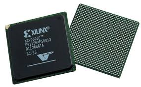
FPGA is most likely to be packaged in a BGA (Ball Grid Array) package type as showed in the below figure. BGA is a very common package type that used widely in various applications. The package balls are clearly on the bottom size of the FPGA and they are connected internally to the FPGA silicon die.


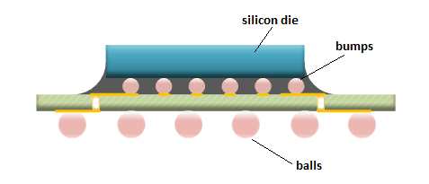
In fact, the package seen above is called Flip Chip Ball Grid Array (FCBGA), and it’s based internally on bumping technology (rather than wirebond technology which is used for smaller size package types). The following figure shows a side view of a BGA package (excluding the top lid)


Picture courtesy of AnySilicon.com


Silicon die – This is the FPGA silicon wafer that has been sawed into a single die. The wafer is produced in a wafer foundry.


Bumps – Those are tiny solder balls connecting the silicon die to the BGA substrate. bumps are distributed across the entire the chip and not only located on the die edge, pads can be placed all over the surface of the die. This allows designers to place more pads per area, reduce the chip size, and optimize for signal integrity.


BGA Substrate – This is the internal PCB that fans out the bumps signals into a larger area and connecting those signals to the balls. The substrate is a small PCB located inside the package and is very similar to other PCBs. The main difference is the BGA substrate size, via, routing are much smaller than most of the PCBs you have seen before.


Balls – Those are the solder balls that connect that BGA package to the target application PCB.


Lid – Is the top surface that is commonly used for company logo and part number is actually used for protecting the die from physical damages and also to dissipate the heat generated by the silicon die.

linked in icon
Sign up for HardwareBee
* = required field

Recent Stories

5+ Best UWB Chipset Providers Compared
SPARK Microsystems Announces CDN$48 Million Financing Led by Idealist Capital
What is MicroLED? Overview, Benefits and Future
Auto processor market growing at 13% CAGR 22-28
The Ultimate Guide: Current Mirror
What is the Difference: GDDR5 VS. GDDR6
Watt to dBm (free) Converter
dBm to Watt (free) Converter
Get 3 Quotes from Electronic Design Companies
Get 3 Quotes from FPGA Design Companies
Get 3 Quotes from Embedded SW Services
Get 3 Quotes from EMS Companies

Find Design Services

Get Price Offers From
  • Electronic Design Services
  • FPGA Design Services
  • Embedded Software Companies
  • PCB Layout Services
  • Printed Circuit Board Manufacturers
  • Design & Manufacturing Services
Welcome New Vendors
  • Cologne Chip – GateMate
  • SPARK Microsystems – SR1000
  • TrigoPi
  • Fidus Systems
  • PCB Design
Answer a Question
  • Tips For Installing a PCB Prototype Board
  • Benefits of Working With a Reliable Flex Printed Circuit Board Manufacturer
  • FPGA company gross margin?
  • What is an FPGA used for?
  • When was FPGA invented
Recent WikiBee Items
  • FPGA Synthesizer
  • FPGA Logic Analyzer
  • FPGA Prototyping
  • Resistivity Definition
  • Inductive Reactance Formula
Recent Posts
  • 5+ Best UWB Chipset Providers Compared
  • SPARK Microsystems Announces CDN$48 Million Financing Led by Idealist Capital
  • What is MicroLED? Overview, Benefits and Future
  • Auto processor market growing at 13% CAGR 22-28
  • The Ultimate Guide: Current Mirror
Most Popular Blog Posts
  • Promwad Accelerates Product Development with Vendor-Agnostic FPGA Design in Multiple Industries 
  • Understanding Knee Voltage
  • Understanding UPS Block Diagram
  • Understanding DV/DT in Electronics
  • Understanding Charge Pump

Never miss an update!

Follow us on LinkedIn

Do you need any price
information?

(Electronic design, FPGA design, Embedded SW services, PCB design, Turnkey)

Yes
No
HardwareBee

Copyright 2017-2023, HardwareBee. All rights reserved.

  • About Us
  • Contact
  • Subscribe
  • News
  • Get Free Support
  • Get listed
  • Send a wiki/article
  • Advertise

Follow Us

Be sure to follow our LinkedIn company page where we share our latest updates LinkedIn
Partner with us Partner with us

Design and Manufacturing Services

  • Engineering Design Services
  • Electronic Design and Manufacturing
  • Electronic Product Development
  • Electronic Product Design
  • Electronic Consulting Services
  • Electronic Engineering Companies
  • Electronic Engineering Services
  • Electronic Product Design and Development
  • Electronics Design Services
  • Electronics Design Company
  • Electronic Design Consultants
  • Electronic Design Company
  • FPGA Design Company
  • FPGA Consultant
  • FPGA Design Services UK
  • Electronics Manufacturing services
  • Electronics Manufacturing Companies
  • Electronic Contract Manufacturing Companies
  • Electronic Manufacturing Services Companies
  • EMS Companies Directory
  • Electronic Design Services
  • FPGA Design Services
  • Embedded Software Companies
  • PCB Layout Services
  • Printed Circuit Board Manufacturers
  • Design and Manufacturing Services