
Buck Boost Converter
22/11/2021, hardwarebee
The ecosystem of switched-mode power supplies (SMPS) is a wide jungle with several different animals: the buck, the boost, the fly-back, the half-bridge, among others. Although the topology and application can vary greatly, they all share a common trait: the ability to precisely change the level of a voltage source while maintaining an efficient and controlled power flow. The SMPS achieves that by using switches to periodically swing power between reactive components, such as inductors and capacitors, using their dynamics to obtain and filter the desired voltage level. The value of the output voltage is therefore a function of the duty-cycle of the switching signal. In this article, we will present the buck-boost converter, which is a SMPS topology capable of obtaining output voltages both higher and lower than the input supply, making it a very flexible and comprehensive circuit. Here we cover the basic concepts, operation modes and the pros and cons of this converter. Finally, we present the closed-loop buck-boost, which implements control theory to automatically regulate the output voltage.
Basic Concepts
The Circuit
Like the buck and the boost topologies, the buck-boost is a non-isolated power converter. However, the buck-boost is capable to provide a voltage both higher and lower than the input source. To analyze the operation of the buck-boost converter, we will apply the same reasoning used in the Voltage Booster article. The circuit is shown in the Figure 1, and it is interesting to notice that the number of components is the same as the buck and the boost, but the functionality is slightly different: the polarity of the output voltage is opposite to the input.
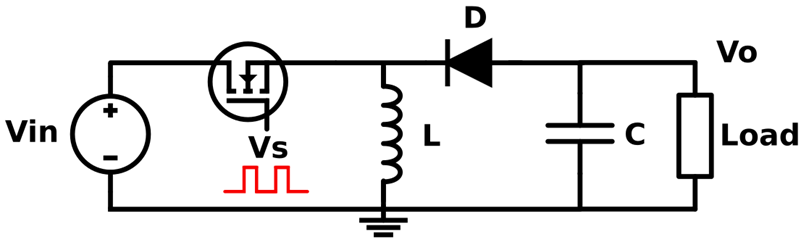
Figure 1: The buck-boost topology
The ON state of the buck-boost converter is very similar to the boost: the input voltage charges the inductor and stores the energy in the magnetic field (Figure 2). In the steady-state operation, the inductor current grows linearly, directly proportional to the input voltage and inversely proportional to the inductance. The diode isolates the input voltage from the output, while the capacitor is responsible for maintaining the output voltage. The voltage VO decreases with the RC time constant, so the voltage ripple depends on the capacitor. The output voltage during this step is:
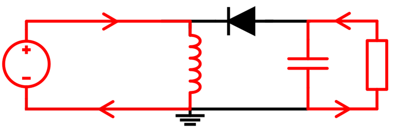
Figure 2: Switch ON State
When the switch opens, it breaks the connection between the input voltage and the inductor. As the stored magnetic field prevents the inductor from changing the current value and direction abruptly, this current starts to flow through the load and capacitor. The inductor voltage, on the other hand, inverts to comply with the output voltage. Thus, during the OFF state, the inductor powers the load and charges the capacitor, recovering the output voltage back to the initial value. Meanwhile, the inductor current drops linearly, with the slope being proportional to the output voltage. In the steady-state operation, this current drops to the initial value of the ON state. The load voltage during this step is:
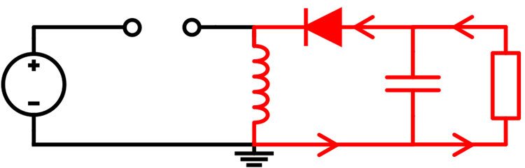
Figure 3: Switch OFF State
Qualitative Analysis
Therefore, the buck-boost operates by storing energy inside the inductor and transferring this power to the right side of the circuit. Therefore, it is reasonable to assume that the output voltage will be proportional to the duty cycle: a duty-cycle equals to 0 means that the input voltage is never connected to the inductor, resulting in a zero output voltage. As the duty cycle increases, the inductor is capable of receiving more energy from the input, and the output voltage increases. To understand intuitively the relationship between input and output, remember that:
- The slope of the inductor current depends on the inductor voltage and inductance;
- In steady-state regime, the inductor current at the end of the OFF state always returns to the same value at the initial of the ON state.
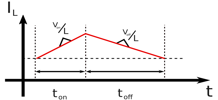
Figure 4: Understanding the buck-boost ratio
Therefore, with the increase of the duty-cycle, the ratio between the ON and OFF time increases, so the current slope must also increase to return to the same point. If the inductance remains the same, this compensation is provided by an increase in the output voltage. For instance, with a duty-cycle of 50%, the inductor spends the same time charging and discharging, so the slope is the same and VIN = VO. It is important to emphasize that this qualitative analysis only works in the steady-state regime; otherwise our second assumption is not correct. During the transient phase, the average inductor current increases with the output voltage. Because the output voltage decreases this current (negative slope), an equilibrium point is eventually reached, ending the transient regime.
Operation Modes
Continuous Conduction Mode
Similar to other SMPS topologies, the buck-boost has two basic operations: the continuous conduction mode (CCM) and the discontinuous conduction mode (DCM). Both CCM and DCM refer to the inductor current. When operating in CCM, the current never reaches zero, so it begins the ON state from an initial value and, after reaching the peak, it returns to the initial point (Figure 5). Thus, there is always current flowing through the inductor.
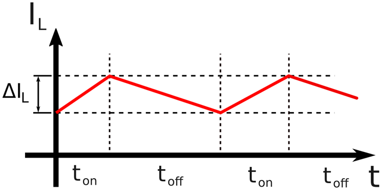
Figure 5: Buck-boost operating in CCM
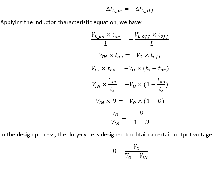
From the waveform and the analysis discussed in the previous section, we can easily find the transfer function by matching the current variation during the ON and OFF states:
Discontinuous Conduction Mode
In the discontinuous mode (DCM), the energy transferred to the inductor during the ON time is not enough to maintain the current flowing during the complete OFF state, which forces the inductor current to reach zero at a certain point (Figure 6). The presence of a dead-time that depends on the duty-cycle prevents us from using the analysis used in the CCM case.
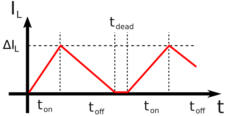
Figure 6: Buck-boost operating in DCM
The output voltage can be obtained by calculating the output current IO, which is equal to the DC diode current (as the capacitor does not allow DC current flow). The equation below describes the output voltage in terms of the converter parameters:
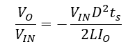
Compared to CCM, the DCM transfer function of D is non-linear (quadratic) and depends on several other parameters, such as input voltage, switching frequency, inductance and load demand. Therefore, it is more difficult to design and implement DCM buck-boosts in open-loop.
CCM versus DCM
At the beginning of the design flow, it must be decided if the converter will operate in CCM, DCM or both. For instance, DCM can occur with light loads, whereas CCM requires higher output currents. There are several advantages when applying each method, which can be used to guide the design:
- CCM
- Lower EMI and ripple;
- Lower current peak efforts for the components;
- Easier to design;
- Does not depend on circuit parameters in open-load;
- DCM
- Lower inductance required;
- Lower switch losses;
- No reverse recovery loss on the diode;
- Easier to control in closed-loop applications;
Advantages and Disadvantages
As mentioned earlier, the buck-boost is both a step-up and step-down converter. So why do we still use bucks and boosts, if they can be replaced by only one circuit? The answer resides on the duck analogy: a duck can fly, swim and walk, but not as good as other creatures that can only do one of these actions. In the same way, the buck-boost is outperformed by the buck and the boost topologies if we only consider the step-up or step-down response. Therefore, before applying the circuit, one should consider its pros and cons.
Advantages
The first obvious advantage is being capable of providing both step-up and step-down conversion. This is essential for applications that require different voltage levels with the same component or a constant regulated output with a varying or unstable input. Moreover, when compared to other topologies, the component count is really low: exactly the same as the buck and the boost converters, which decreases cost and complexity significantly.
Disadvantages
The buck-boost provides an inverted output, which is prohibitive in several applications. Furthermore, the input current is discontinuous, resulting in a poor EMI performance at the input line. For small or large duty-cycles (> 0.7 and < 0.3), the efficiency drops significantly, so it is recommended for middle range gains. Finally, due to the inverting polarity of the output, closed-loop feedback applications require extra complexity to read the value.
The controlled buck-boost
Although the output voltage can be designed with the transfer function equation, it does not ensure that manufacturing errors or environmental conditions cannot interfere with the final value. Moreover, if the transfer function is kept unchanged, the output is prone to input variations. Therefore, a closed-loop solution is often applied. Figure 7 shows the general block diagram that can be applied in the buck-boost. The sensing block reads the output voltage, reducing it to more manageable values. Then, the difference amplifier compares the input reference with the output voltage, generating an error signal. This error signal is fed to the regulator, which implements the control part of the system. A PI or PID controller is usually applied in this stage. Finally, the control signal is converted to a PWM signal that controls a driver. The driver is the interface between the switch and the instrumentation electronics, and it is used to provide more current capability and electrical isolation. If the system is well modelled, the output will remain stable even with large input variations.
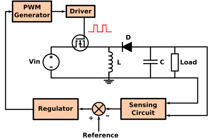
Figure 7: The Controlled Buck-Boost


