
Quiescent Current
04/09/2021, hardwarebee
The current flowing when a circuit is at rest or without load is known as quiescent current (IQ). This is a crucial aspect to remember when constructing battery-powered systems like wireless belt pack transmitters. The overall current drain, which includes both quiescent and loads current, determines battery life. Because most battery devices spend more time in standby mode than in operation mode, quiescent current consumption is the most important factor to consider. To extend the battery’s life, the idle current consumption should be as low as feasible.
Quiescent Current in Semiconductors
The quiescent current has a somewhat different meaning for load switches compared to other semiconductors. The quiet current of the device passes into the ground pin instead of via the pass FET. Second, the typical peace of mind of a load switch is on the micro-amp. This indicates that the calm current is low for an ampere of an mm or higher capacity like an LED, as the calm current is a smaller fraction of the overall power used for the system.
Quiescent current of an LDO
Quiescent current is used when an LDO is activated by the internal control circuit. The current flow from the GND terminal is the Quiescent current. The current from the GND terminal is called a relaxing current. The datasheets show a value for the input voltage selected for VIN, bias voltage (VBIAS), and zero load temperature (IOUT=0A). Low-scale LDOs are excellent for mobile applications with battery power. Figure 1 shows the schematic depiction of quiescent current of an LDO.
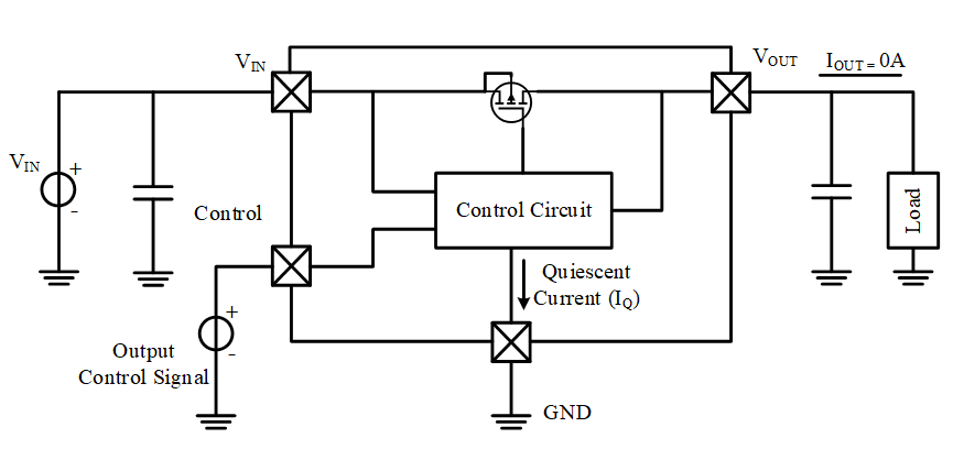
Figure 1: Quiescent Current of an LDO
Quiescent Current of an Amplifier / Transistors
In amplifiers usually, Quiescent current is employed. Amplifiers have a considerable relaxing current as of the output device(s) always have an important current level. When the output is zero, the current level of an amplifier in the amplifier is defined as the quiet current. Class A amplifiers convert the huge quiet current to create a variable current under load, thus they are never inadequate with regard to power.
The voltages and currents present in a transistor circuit while the power supply is on and stable and no signal is supplied characterize the quiescent state. It is important to remember that while DC biasing a transistor for an amplifier, the transistor should be in the active area for the whole range of input signal provided to it. On the VCE-IC load line curve, a fixed quiescent point is set to provide a fully amplified signal at the input. In quiescent current IC is the collector current and VCE is the collector voltage as shown in figure 2. Quiescent current (Q-point) only measure at the center of the load curve.
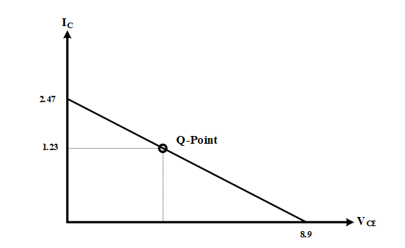
Figure 2: Quiescent Current Curve
Some current sources, resistors, and voltage drive in the transistor quiescent. It allows you to select certain preset DC voltages and currents to work in a specific area for the transistor. When no current is applied to the component, the transistor status is referred to as a DC point, also called a relaxing point.
Quiescent Current Response to Changing Conditions
A load switch’s quiescent current fluctuates depending on various conditions, i.e. supply voltage and temperature.
- As the supply voltage rises, the quiescent current rises as well. Although other load switches have different internal circuit layouts, the charge pump that operates the gate of the FET is usually to blame for the higher quiescent current.
- Temperature affects the quiescent current as well. As the temperature rises, the quiescent current rises as well. This is owing to the control circuitry’s temperature dependence.
Impact of Quiescent Current
The quiescent current impact depends on the following factors:
- During a light load operation, nominal, calming current can have a substantial effect on the power transmission efficiency of the system. Sometimes the Quiescent current gets confused. The system sits inactive with silent current, but will always wake up and act, which is usually how consumers prefer their gadgets. Shutdown current, however, relates to a sleeping device.
- Designers utilize Quiescent current to assess the power consumption at light charges of a power supply. If the device is switched off but the battery is attached to the controller, the battery life is determined via shutdown current. When building a battery life extension device, you always utilize low-energy microcontrollers, sensors, radios, and efficient power sources.
- CMOS manufacturing methods and other design strategies can help lower the total energy consumption of a device that can enhance battery life. Some designers employ a boost converter to prolong the battery life if the battery voltage drops too low. But this technique might lead to a greater calming current that drains the battery quicker unless the correct transformer is used. Another key aspect is the form factor of the finished product.


