
Understanding Anderson’s Bridge
10/05/2022, hardwarebee
This article presents Anderson’s bridge concept, principles, and its applications. This Anderson’s bridge is used for accurate inductance measurement. There are three main inductance measurement techniques in electronics, but this bridge can cover the limitation of the other methods. Alexander Anderson invented Anderson’s bridge circuit in 1891 by modifying Maxwell’s inductance capacitance bridge to give a very accurate measurement of self-inductance. Like other bridge circuits, Anderson’s bridge is also analyzed in a balanced condition.
In this article, the Anderson’s bridge circuit is solved in two ways to determine the unknown inductance in the circuit. One of the questions that may arise for each new measurement technique is why we need this new method when other bridges are already available. To answer this question, the limitations of other methods should be studied because new approaches are defined to overcome the available problems or enhance them. Three important AC bridges for finding the self-inductance of a coil are:
- Maxwell’s inductance bridge
- Maxwell’s inductance-capacitance bridge
- Hay’s bridge
To describe their limitations, it can be said that Maxwell’s inductance bridge needs a large standard variable resistance (R2) to measure a low Q coil. Hence, this technique is not appropriate for low Q inductances. A similar issue is available for Maxwell’s inductance-capacitance bridge, which requires a very large variable resistance (R4) for a low Q inductance. In Hay’s bridge, a large variable resistance is necessary, which increases the costs of the circuit and makes it unsuitable for measuring low Q inductance. Thus, to come up with this problem in low Q coils, Anderson’s bridge was proposed. Before explaining the bridge, the Q factor is discussed in this article.
The Q factor is defined to indicate the quality of the inductor, and it is called the “Quality Factor”. Each inductor has both inductive and resistive behaviors. As copper or aluminum conductors are used in inductor manufacturing, the resistances of conductors must be considered. Hence, the ratio between inductance and resistance is defined as the frequency- dependent quality factor, which can be written as follows:
(1)
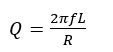
where f is the frequency of the flowing current through the inductor, L and R are the coil inductance and resistance, respectively. The low Q factor represents high resistive loss and low inductance which is unsuitable in terms of quality because the main objective is building an inductor with maximum acceptable inductance and low loss.
Anderson’s bridge circuit consists of four arms to measure an unknown inductance. The circuit diagram is shown in Figure 1. This circuit is quite similar to Maxwell’s inductance-capacitance bridge because Anderson’s bridge is a modified version of Maxwell’s bridge to measure inductances with a low-quality factor (less than 10). The first arm is between nodes A and B, which have an unknown inductance (L1) in series with a non-inductive resistance (R1). Each second and third arm includes a non-inductive resistance, as shown in the figure by R2 and R3. The other arm is also a non-inductive resistance, but there are a variable resistance (R5) and a capacitance (C) in parallel. In measuring circuit, using a detector or meter is necessary to find the balanced condition for the bridge, and in this bridge, a galvanometer is connected between node B and the junction of capacitor and variable resistor, which is called node E. The inductance value can be determined by solving the bridge in a balanced condition. It means that the meter must show zero current in BE path.
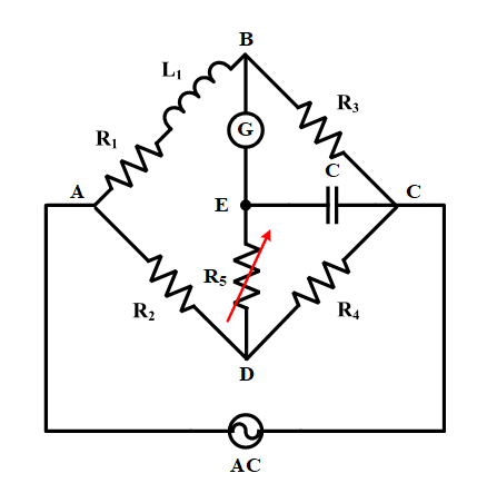
Figure 1: Anderson’s bridge circuit configuration for measuring unknown inductance
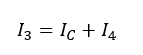
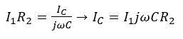
To analyze the circuit, currents in bridge paths should be named, and then use Kirchhoff’s Laws to find the value of unknown inductance in the first arm. To write Kirchhoff’s current law (KCL), currents in the paths are illustrated in Figure 2. Assume the bridge is in a balanced condition, the current in path BC is zero, and currents in DE and EC are the same (IC). Moreover, I1 flows in AB and BC, and the voltages of arms are E1, E2, E3, and E4.
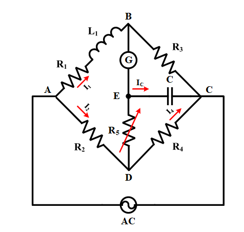
Figure 2: Current paths in Anderson’s bridge
Based on Kirchhoff’s current law, the following equation can be written.
(2)
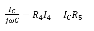
Then, Kirchhoff’s voltage law (KVL) must be written in different loops. In loop BCEB, the KVL can be presented as:
(3)
In loop ABEDA, the KVL equation would be as:
(4)
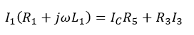
The KVL is presented in loop BCDEB as:
(5)
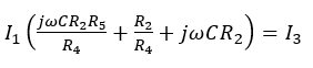
By Equations 2 and 5, the following equation is obtained.
(6)
![]()
Then, the capacitor current can be replaced by Equation 3, and the output would be:
(7)
Now, this sequence can be executed for Equation 4 by using Equation 3. The result would be as below:
(8)
![]()
Considering Equation 7, the equation 8 can be re-written as given:
(9)
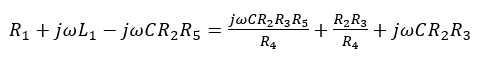
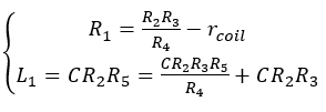
Finally, the real and imaginary parts of Equation 9 express the resistance and inductance of the first arm of the bridge, respectively. These parameters can be calculated as follows:
(10)
Since this bridge is proposed to measure the low Q inductors, a coil resistance can be considered in the circuit in series with coil inductance and R1. Therefore, the modified version of Equation 10 would be:
(11)
The inductance and resistance of the first arm can be achieved by the presented method. However, the circuit can be solved by the star-delta conversion technique, which will be explained in the following parts of this article. The star-delta conversion is a technique to solve complex impedance configurations, especially when the impedance is neither series nor parallel. As can be seen in Figure 3, any delta connection can be converted to an equivalent star configuration and vice versa. Therefore, the values of impedances must be calculated based on the conversion. When the circuit is in delta connection, the equivalent star impedances can be obtained by:
(12)
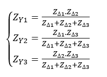
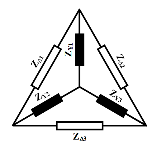
Figure 3: Star and delta impedance configurations
In Anderson’s bridge, there is a delta configuration (ECDE) which can be converted to the star connection using Equation 11. As shown in Figure 4, the equivalent impedances in star connection can be calculated easily as below:
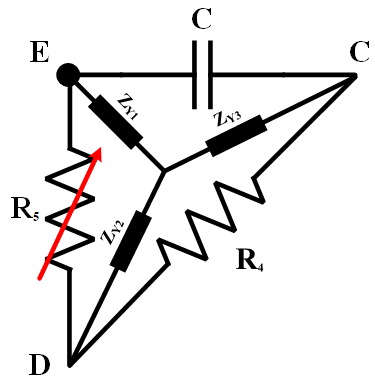
Figure 4: Equivalent star circuit for ECDE path
(13)
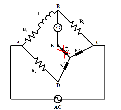
Figure 5: Modified circuit based on the star-delta conversion
The equivalent star circuit is replaced by the delta connection, as shown in Figure 5. In the balanced condition, no current flows in the galvanometer. Thus, the series impedance with the meter can be neglected because its flowing current is zero. In this situation, there is a balanced bridge, and the following criterion is valid.
(14)
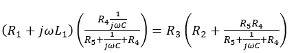
![]()
By Equation 12 and 13, the given equation is achieved as:
(15)
By canceling common parts and separating the real and imaginary parts, the resistance and inductance of the coil can be obtained as:
(16)
which is exactly similar to Equation 10.
After determining the relation between Anderson’s bridge components, the phasor diagram of this configuration can be helpful for better understanding. For this purpose, the input AC voltage is considered a reference voltage. Then, the phasor of current I1 must be plotted, which flows through L1 and available resistances in the path of ABC. As I1 is an inductive current, it lags the input voltage, and the voltage across the inductance (jwL1I1) will start from node A with a 90 degrees phase angle difference with respect to the current. To reach nodes B and C, the voltages across the resistances must be plotted, as shown in Figure 6.
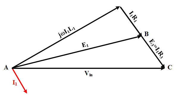
Figure 6: Phasor diagram of ABC path in Anderson’s bridge
In a balanced condition, nodes B and E are identical. It means that the voltage across R3 is equal to the capacitor voltage. The capacitor current leads the voltage so that the phase angle between voltage and current would be 90 degrees. The voltage across the variable resistance is also based on capacitor current as the bridge is in a balanced condition. The current in the fourth arm starts from node C and ends at node D, as depicted in Figure 7. Finally, the voltage of the second arm can be drawn from node A to node D.
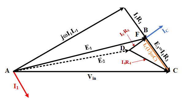
Figure 7: Complete phasor diagram of Anderson’s bridge circuit
To wrap up the article, the pros and cons of this bridge are discussed. The cost of a standard variable resistor in this bridge is low, and a fixed capacitor can be used. Hence, this bridge is economical. The capacitance can also be determined if the inductance is known. Moreover, the balanced equation is independent of which makes the bridge stable, and sinusoidal excitation is not necessary. In contrast, Anderson’s bridge is more complex compared to Maxwell’s bridge and have more components. Furthermore, this bridge is not suitable for high-frequency applications because it is difficult to shield as a junction has been added to the circuit compared with Maxwell’s bridge.


