
FPGA Design Flow – An Introduction
02/04/2018, hardwarebee
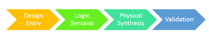
The design flow of Field Programmable Gate Arrays (or FPGAs) consists of several steps that must work in unison for proper function. The steps consist of the following:
- Design Entry
- Logic Synthesis
- Physical Synthesis
- Verification
- Implementation
Each step must be followed and verified to ensure that the FPGA design is functioning according to its design parameters. It is true that some manufactures may add certain steps to the process, but the overall creation of the design process follows these guidelines.
Design Entry
This establishes the requirements, architecture, and function of the FPGA. The result is a design that can be simulated for functional verification, if possible, before the synthesis process can begin. The design is created, some other design files added, and any constraints to the pin, area, or timing are put into place. The entry is now tested using different models to ensure that it behaves as expected. Once completed, the FPGA design process reaches its next step, synthesis.
Logic Synthesis
This is the point where the design is synthesized which calls for the conversion of the HDL description to a written design circuit schematic sometimes called a netlist. A special software is used to perform the function of synthesis. If the HDL code is correctly written, then the FPGA should pass without issues. However, the synthesis process may reveal some issues or possible errors that got past the initial testing process. Any errors must be addressed by the FPGA engineer before going to the next step.
Physical Layout
Once synthesis is completed and the FPGA design has passed, the next step is implementing the design onto the internal structure of the device itself. This is called layout or place and route, that allows the resources of the FPGA, such as the connection wires, logic cells, and the like, to be put into their proper place. Once established, the FPGA is ready to be tested in the lab – so the verification phase should be initiated.
Validation
The FPGA is put through a final verification process after the mapping and place and route has occurred. This means that it’s time to go to the lab, download the FPGA code into the FPGA and test the FPGA functionality in real life. Depending on the FPGA complexity, the validation process may be a short or lengthy one depending on the overall quality of design and testing methods that are used.


