
Introduction to Analog Design
02/12/2020, hardwarebee
Before digital electronics have been invented, all devices worked with analog circuits. Analog circuits represent the real world because we live in an analog world where all waves (sound waves, electromagnetic spectrum waves, voltage and current waves) are analog signals. Therefore, an analog signal represents a variation of a continuous variable from our physical worlds such as current and voltage signals contrary to a digital signal which can only represent logic 1 or logic 0 value.
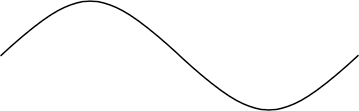
Figure 1: Analog sinusoidal electrical signal in an AC circuit
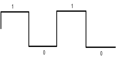
Figure 2: Digital signal
Practically, an analog design includes both passive and active components such as capacitors, resistors, inductors, transistors, diodes and operational amplifiers (op-amp).
In this article, we will talk about principal analog design that can be found in all most today’s printed circuit boards (PCBs). Read and learn about the most popular analog design blocks that appears in almost every electronic design.
Oscillator
Oscillators can produce a continuous, periodic alternating waveform or signal that has a constant peak to peak amplitude. The produced signal may be a sinusoidal, a triangle or square wave. This signal generator produces signals without any input signals except the power supply signal to get sustained oscillatory output. The output frequency can be either fixed or variable according to the oscillator design.
Generally, oscillators can be classified as:
- Sine wave oscillators which produce a sinusoidal signal using a combination of resistor, inductors and capacitors or crystals to build resonators which are represented in Figure 3.
- Astable multivibrators and relaxation oscillators which generate rectangular pulses and square waves.
- Sweep oscillators generate sawtooth waves output.
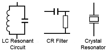
Figure 3: Different type of resonators
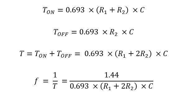
In this case, we will explain one of the most important oscillators using the famous integrated circuit (IC) NE555 as an astable multivibrator to control and light on alternatively two LEDs at a certain frequency tuned using resistors. This circuit can be also used to produce pulse width modulation (PWM) to monitor a DC motor at a certain frequency.
The astable 555 oscillator circuit is represented in Figure 4, where both pin 2 and pin 6 are linked together to re-trigger the circuit on every new cycle. In each cycle, the capacitor (C) will be charged up via both R1 and R2 resistors and will be discharged via R2 resistor which is linked with pin 7 (i.e., the discharge pin). Pin 3 represents the output voltage applied to LEDs that we want to control.
Therefore, the capacitor (C) will be charged up to 2/3Vcc within the 0.693(R1+R2)C time combination and the capacitor will be discharged to 1/3Vcc within 0.693(R2*C) combination time. This circuit will produce a periodic square wave with an amplitude of Vcc – 1.5 volts.
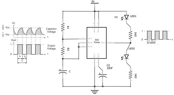
Figure 4: Astable 555 oscillator
The important formulas which permit to calculate different parameters of the astable 555 oscillator such as the frequency of the output square wave are listed here
Phase-Locked Loop (PLL)
The phase-locked loop (PLL) is a very important circuit block in a linear system. PLL can be employed in many applications like satellites, radars, stable clock generator for microcontrollers, FM/AM demodulator, frequency division/multiplication, frequency synthesizer, radio frequency and wireless applications.
A PLL mainly has three important blocks represented in Figure 5:
- Phase detector block detects any difference between the input signal frequency fin and the feedback output signal frequency fout and then generates a proportional DC error voltage to the phase difference which is applied to the low pass filter. Practically, the phase detector is a signal multiplier that generates two frequency components at its output, i.e, the sum of frequencies (fin+fout) and difference of frequencies (fin-fout).
- Active low pass filter generates a DC voltage at its output and removes the high-frequency component the phase detector output and amplifies the signal.
- Voltage Controlled Oscillator (VCO) produces a signal with an output frequency which is adjustable to meet the input frequencies and proportional to the DC output voltage of the active low pass filter.
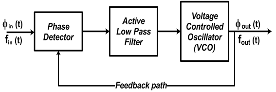
Figure 5: PLL diagram
Therefore, we present the IC 565 which can be used to achieve the PLL scheme. IC 565 can operate at a voltage range from ±6 volts DC to ±12 volts DC and has 14 pin Dual-Inline Package (DIP) where only 10 pins (pin 1 to 10) are useful and the four other pins (pin 11 to 14) aren’t connected ( labelled with NC,i.e., No Connection). The pinout diagram of IC 565 is represented in Figure 6.
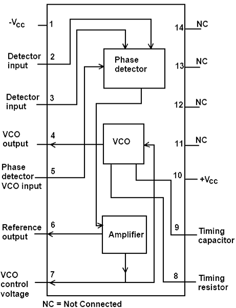
Figure 6: Pinout diagram of IC 565
The output of VCO is generated at pin 4 while pins 2 and 3 are grounded. The output frequency of the VCO is expressed as:
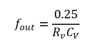
- Rv : the external resistor which is connected to the pin 8
- Cv : the external capacitor which is connected to the pin 9
Pins 4 and 5 should be shorted with an external wire to apply the output of VCO to one of the phase detector inputs.
Therefore, the IC 565 provides an internal resistance of 3.6 Kiloohms (R2) to build the low pass filter by adding a capacitor (C2) between pin 7 and pin 10 as shown in Figure 7.
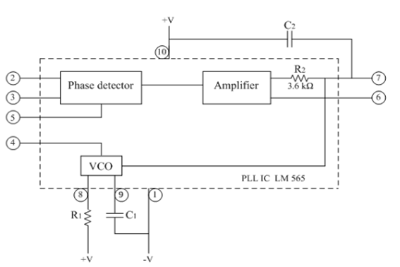
Figure 7: PLL IC 565 wiring diagram
Digital to Analog Conversion (DAC)
The Digital to Analog Converter (D/A, DAC, D2A) is an electronic device that permits to converts binary logic values (0 and 1) to a set and group of continuous analog voltages. DAC is usually used in various applications mainly when converting digital signals such as audio waves transmitted from a computer to other devices like speakers which need understandable analog voltages.
In the other hand, the digital to analog conversion is a scaling operation where the binary representation is mapped and corresponds to a certain voltage range. Figure 8 shows a DAC that accepts 3 binary bits as input and provides 23=8 outputs.
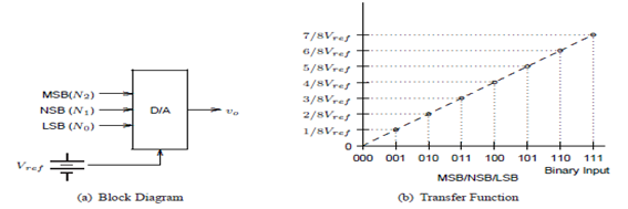
Figure 8: 3 bit DAC
The general mathematical representation of a D/A conversion process can be summarized using the following formula where 0V corresponds to the minimum and the maximum voltage (reference voltage) corresponds to the maximum input binary value :
- Vo is the Output Voltage
- Vref is the Reference Voltage
- N is the Input binary value
- M is the Number of binary digits input
There exist various techniques to implement DAC circuit. The first one is the easiest one by using R-2R (3 bits) ladder DAC network as represented in Figure 9.
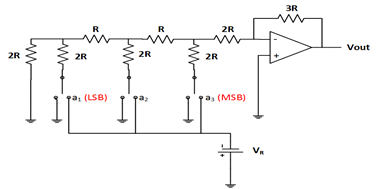
Figure 9: R-2R ladder DAC
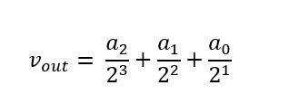
To sum up, the binary input values will be going into the 2R resistors and the voltage output will be obtained at the bottom of the ladder. The voltage output is calculated according to the following formula and can also be applied to other DAC with a higher number of inputs bits.
In the other hand, you can build a DAC from a microcontroller using PWM signal. You have to add an RC low pass filter to filter the AC component and convert the PWM signal into a DC voltage value as depicted in Figure 10. The voltage value is the PWM mean value which is related to the duty cycle (ratio of on-time to period). The mean value is obtained by adding the RC filter stage.
There are many popular DAC IC in the market such as MCP4725, DAC0832, DAC7715, DAC0808 etc…
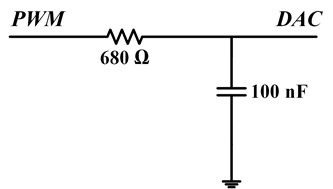
Figure 10: Building a DAC using the PWM signal and the RC filter
Analog to Digital Conversion (ADC)
An analog to digital converter (ADC, A/D) is a device that can convert a continuous analog voltage value to a digital binary logic value (0 or 1) which is understandable by a digital device such as microprocessor or microcontroller. We can convert temperature, pressure, sound, light, speed, etc… to digital values using a simple ADC by mapping voltage values to binary values as shown in Figure 11.
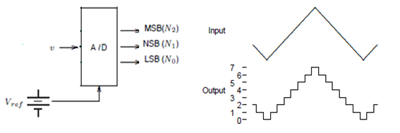
Figure 11: A/D conversion
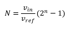
There exist many ADC ICs in the market like ADC0808, ADC0804, ADS1115, MCP3008 etc… The general rule of thumb of ADC is that the voltage value is scaled to a binary value and the maximum binary value obtained represents a voltage which is called is the reference voltage. The logic values are obtained according to the following formula:
Where,
- Vin is the Input Voltage of the ADC
- Vref is the Reference Voltage
- N is the Output binary value
- n is the bits Number of ADC
In Figure 12, we will present the wiring diagram of IC ADC0808 which is employed to convert sensor temperature data (LM35) connected to IN0 (channel 0) into digital values of 8 bits (pins OUT1 to OUT8).
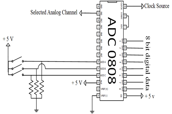
Figure 12: Wiring diagram of LM35 with IC ADC0808
Analog Filters
Analog filter is considered as the basic principle block which is used in electronics for signal processing to remove or attenuate undesirable portions from the desired signal. Analog filters are mainly employed in radio frequency (RF) applications to select a desired radio station from the received signal for example or to filter an audio signal before entering to loudspeakers.
Analog filters generally use passive linear electronics components such as inductors, resistors and capacitors to attenuate or reject particular frequencies from the continuous-time signal.
In this section, we discuss different types of linear analog filters such as Butterworth filter, Chebyshev filter and simple filters.
Butterworth Filter
The Butterworth filter is known as a maximally flat magnitude filter (in the brick wall region) that provides a flat frequency output response that is improved by increasing the order of the Butterworth filter as shown in Figure 13.
The Butterworth filter can be designed using either Sallen-key or Cauer topology which are represented in Figure 14 and Figure 15 respectively.
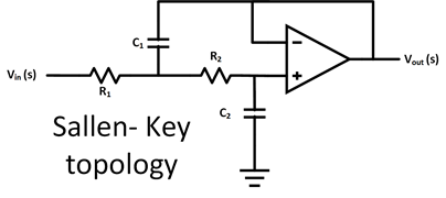
Figure 13: Sallen-Key topology
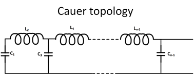
Figure 14: Cauer topology
Simple Analog Filters
RC filter
The RC filter is considered as the simplest circuit in the analog design. This circuit plays a role as an analogue filter to filter signals by blocking certain frequencies and allowing others. The RC filter can be designed as either a series or parallel RC circuit as depicted in figure 15.
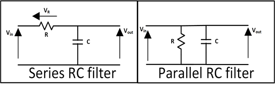
Figure 15: RC filter
LC Filter
The inductor-capacitor (LC) circuit is a filter and is known as a tuned, resonant or tank circuit. The LC circuit acts as an electrical resonator to generate signals or to extract signals at the desired frequency. The LC filter can be designed as either a series or parallel LC circuit as depicted in figure 16.
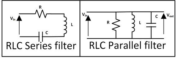
Figure 16: LC filter
RL filter
The resistor-inductor (RL) circuit behaves as a filter which can be designed as either series or parallel RL circuit as depicted in Figure 17.
Figure 17: RL filter
RLC Filter
The resistor-inductor-capacitor (RLC) circuit behaves as a filter which can be designed as either series or parallel RLC filter which acts as a harmonic oscillator and resonates as an LC filter where the oscillations can be damped or decayed by adding a resistor component as shown in Figure 18.
Figure 18: RLC filter
Decoupling Capacitors
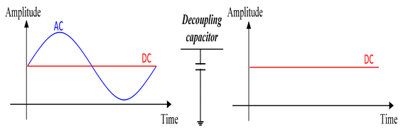
Figure 19: Decoupling capacitor role
In general, the decoupling capacitor is defined as a capacitor that is used to suppress AC components from a DC waveform signal. This type of capacitors is employed in many circuits to vanish noise in a DC power source as shown in figure 19.
The decoupling capacitor is a ceramic capacitor type with a value of 10 nF to 100 nF placed in parallel with the power supply as depicted in figure 20. In the other hand, they also can be employed with logic chips such as microcontrollers where there are high switching components from the low state to the high state like push buttons to remove transient voltage spikes.
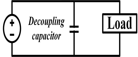
Figure 20: Decoupling capacitor in a power supply
Operational amplifiers (Op-amp)
An operational amplifier (op-amp) is a voltage amplifying circuit that can be employed with passive components like resistors and capacitors between the input and the output terminals. Op-amp is considered as the hearth of analog devices and it is a linear device that can be used to perform amplification, filtering and many mathematical operations such as subtraction, addition, integration and differentiation.
The op-amp offers the feedback process which is considered as one of the most important principles in engineering mainly the negative feedback. The symbol of the op-amp is shown in figure 21.
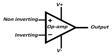
Figure 21: Op-amp symbol
Regulators
Linear regulators are generally used in applications which don’t require high-efficiency, generate a low quantity of heat with low cost and short design time. These are very used in many applications where the output voltage is less than 40 volts DC. This technique permits to produce a single output voltage which is lower than the input voltage. the linear regulator provides an average efficiency of 35 to 50 per cent. However, the energy losses are dissipated as heat.
Recently, regulators are in the form of integrated circuits (ICs) with either fixed positive or negative voltage regulators.
The most employed voltage regulators are 7800 series and integrated circuits will be like IC 7805, IC 7812 and IC 7815 etc. which offer output voltages of +5 volts, +12 volts and +15v. Figure 22 represents the IC 7815 to provide a fixed positive voltage of 15 volts where capacitors C1 and C2 are decoupling capacitors.
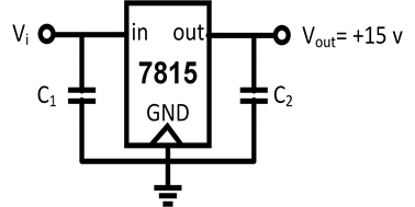
Figure 22: Fixed positive voltage regulator
In the other hand, the most employed negative voltage regulators are 7900 series and integrated circuits will be like IC 7905, IC 7912 and IC 7915, etc… which offer output voltages of -5 volts, -12 volts and -15 volts respectively. Figure 23 represents the IC 7915 to provide a fixed negative voltage of -15 volts where capacitors C1 and C2 are decoupling capacitors.
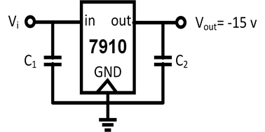
Figure 23: Fixed negative voltage regulator
Serializer/Deserializer (SerDes)
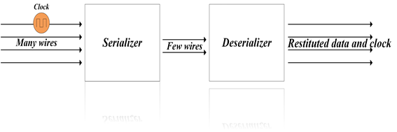
Figure 24: SerDes diagram block
The serializer/deserializer (SerDes) device converts and transforms parallel data into a serial data that through a high-speed connection such as low-voltage differential signaling (LVDS) to a receiver which converts the received serial data back both clock and the original parallel data as depicted in Figure 24.
SerDes has emerged as the primary solution in chips where there is a need for fast data movement and limited I/O, but this technology is becoming significantly more challenging to work with as speeds continue to rise to offset the massive increase in data.
One other important key to the usefulness of SerDes is that contains embedded functional blocks in a single chip that converts parallel data into serial data in high speed without increasing the number of pins.


