
Understanding Quiescent Current
14/05/2022, hardwarebee
The amount of current utilized by an IC when it is in the Quiescent state is referred to as Quiescent Current. The Quiescent state refers to any period of time when the IC is either no load or non-switching but is still switched on. When the external load current is zero, Quiescent Current is also the current required to power the internal circuitry of a low-dropout (LDO) IC.
Quiescent current is sometimes mistaken with shutdown current, which is the current drawn when a device is switched off while the battery is still attached to the system.
The amount of Quiescent Current is affected by the design of the device, the input voltage, and the temperature.
When no load is applied, IQ = IIN. The IQ refers to the power consumption of a power supply in standby mode, which is also known as the quiet condition of a circuit. The circuit’s quite state occurs when the inputs are not cycling and the power source itself is not driving a load. During light-load operation, quiescent current, which is nominal, can have a considerable impact on a system’s power-transfer efficiency. It is important to guarantee that during the DC biasing of a transistor for an amplifier, the transistor remains in the active region across the whole range of input signal delivered to it. A fixed quiescent point is placed on the V(ce)-I(c) load line curve to acquire the entire amplified signal as of the input. Quiescent current and voltage are used to describe the current IC (collector current) and voltage VCE (collector to emitter voltage) at this moment.
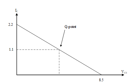
Figure 1: Load Line of an Amplifier
Amplifiers with Quiescent Current
The saturation current (IS) is really important to decide the quiescent current as it should be half of the IS, for any class of amplifier. The halfway is defined as the point between saturation and cutoff. Some amplifiers have zero quiescent current, because they are designed to be cut-off when no signal is provided such as Class B and Class C. Some amplifiers have very low quiescent current, like Class AB. The values of quiescent current are just above the cutoff region. To highlight the range of function for one class of amplifiers, a load line is drawn across the characteristic’s curves of a transistor, this all is done in a state when the transistor is coupled to a specific load resistance. Typical curves of such a case is shown in the diagram below:
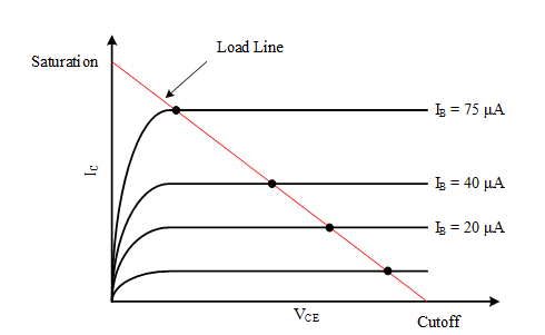
Figure 2: An example load line is shown over transistor characteristic curves
A typical load-line is plotted using the collector currents and the voltage across collector and emitter terminal of a transistor. A cut-off is a state where there is now voltage across the terminals and the current is zero in this situation. The line is saturated because the voltage is zero and the current is largest in the upper-left corner. Actual operating scenarios for the stated base currents are shown by the dots at the intersections of the load line and the different transistor curves.
A single dot along the load line on this graph might signify quiet operation conditions. The middle of the load-line represents the quiescent point (Q-point) as shown in figure below.
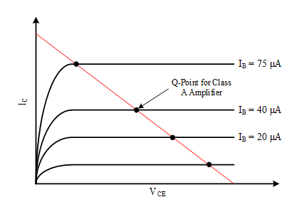
Figure 3: class A Quiescent point (dot)
With a base current of 40 A, the quiescent point in this diagram lies on the curve. The change in the load resistance will also affect the slope of the load-line. The higher load resistance does not have any effect on the cutoff voltage of collector and emitter, while it will only affect the maximum collector current drawn at saturation. When the load-line is plotted for increased resistance, it does not have any effect on the lower-right point while the upper-left point is shifted depending on the load.
Take notice of how the new load line does not touch the 75 A curve at its flat point like the previous one did. It is vital to know that, in a characteristics curve, the saturation condition is indicated by the non-horizontal line. If the load line crosses the 75 A curve outside of its horizontal range, the amplifier will be saturated at that level of base current. After changing the load resistor value, the load line intersected the 75 A curve at this new location, implying that saturation will occur at a lower base current value than before.
A base current of 75 A would result in a similar collector current with the old, lower-value load resistor in the circuit (base current multiplied by). A base current of 75 A produced a collector current almost twice as large as that produced at 40 A in the first load line graph, as predicted by the ratio. Because the transistor loses enough collector-emitter voltage to regulate collection current between base currents of 75 A and 40 A, collector current climbs little.
In order to ensure linear (no-distortion) functioning, transistor amplifiers should not be employed in areas where the transistor would saturate, that is, at locations where the load line does not theoretically rest on the horizontal section of a collector current curve. A couple additional curves have been added to the graph in Figure below to establish how far this transistor can function with higher base currents before saturating.
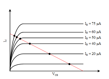
Figure 4: More base current curves reveal saturation information
The highest-current point on the load line falling on a straight section of a curve in this graph appears to be the point on the 50 A curve. This new point should be considered the highest permissible input signal level for class A operation. In addition, the bias should be modified for class A operations such that the quiescent point is in the midway of the cutoff and the new maximum point, as shown in figure below.
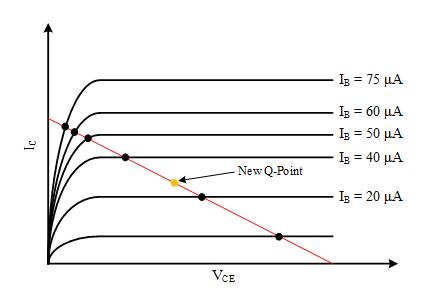
Figure 5: Saturation zone is entirely avoided by the new quiescent point
It’s time to look at some practical biasing approaches. To bias the amplifier for the chosen class of operation, both DC (battery) and AC sources are connected in such a way that AC signal is in series with the DC voltage source. In reality, it’s difficult to connect a perfectly tuned battery to an amplifier’s input. Even if a battery could be custom-made to provide exactly the proper amount of voltage for each specific bias need, it would not be able to maintain that level continuously. When the amplifier started to deplete and the output voltage dipped, it began to operate in class B mode.
Consequences of IQ
The IQ of an LDO regulator, which is used for regulation, is critical for battery life. Because battery life is strongly reliant on load conditions while running, LDOs with low IQ give an easy way to increase the life of a battery-powered device. These teeny-tiny devices aren’t only for consumer electronics. They might also be utilized in industrial applications such as smart meters, building, and factory automation. Even if designers overlook quiescent current on sometimes, running it for a few seconds, days, or even years longer may have a substantial influence on the design.
Types of Amplifiers and their Operations
- Class A: Class A operation refers to an amplifier that is biased to run in the active mode throughout the duration of the waveform cycle, authentically reproducing the whole waveform.
- Class B: In Class B mode, an amplifier is biased such that it can duplicate the negative or positive half of the input waveform. In this class of the amplifiers, the transistor is in active mode half of the time and cutoff mode the other half. Whenever there is requirement of high-power amplification in audio signal systems, the complementary pairs of class B transistors are used. As mentioned earlier, the transistors work in pairs, so each transistor handles the half of the waveform. With the same output power, a class B amplifier has a greater power efficiency than a class A amplifier with the same output power.
- Class AB: Talking about the operation of the Class AB amplifiers, they lie in middle of Class and B amplifiers.
- Class C: Only a small section of the waveform may be magnified by Class C amplifiers. The transistor spends the bulk of its time in cutoff mode. A resonant tank circuit is widely used as a “flywheel” to extend oscillations for a few cycles after each “kick” from the amplifier in order to generate a full waveform at the output. In a class C amplifier, power efficiencies are high since the transistor is not conducting for the majority of the time.
- Class D: The concept of representing instantaneous input signal amplitude by the duty cycle of a high-frequency square wave underpins Class D operation, which necessitates a complex circuit design. There are only two modes of operation for the output transistor(s): cutoff and saturation. Energy efficiency improves when heat energy is dispersed less.
To provide DC bias voltage on the input signal, which is required for certain types of operation, a voltage divider and coupling capacitor can be utilized instead of a battery connected in line with the AC signal source (particularly class A and class C).


