Ultimate Guide: Power Supply Design
19/10/2020, hardwarebee
Power supply design plays a very important role within an electronic and embedded system. In this paper, we will discuss the history of power supply, 3 types of power supply designs, power supply topologies and power supply design consideration.
Power supplies appeared with tethered systems which are linked with electrical wire to a fixed electrical installation to transform, rectify and regulate the alternating current (AC) 110 volts/220 volts to another electrical form, +12 volts/+ 5 volts direct current (DC) which will be used by different system modules.
Power supplies were commonly used and developed as a standalone integrated module in a personal computer (PC) that converts the AC power into many different DC voltage drops to supply other submodules using different electronic parts such as transistors, electrolytic capacitors and magnetic-core inductors. In Figure 1, +12 V, –12 V, and 5 volts DC voltages are drawn from AC power to serve microprocessor motherboard or the hard disk drive.
Figure 2 represents a PC motherboard where the microprocessor, peripheral cards and memory are embedded and supplied the previous power supply unit seen in Figure 1. This power conversion at very near the receiving device is known as a point of load (POL) power conversion.
This idea was introduced in the time of the war of currents between the engineer Serbian-American Nikola Tesla and the American inventor Thomas Edison, while Tesla had proved the possibility of remotely transporting AC power at very high voltages. Therefore, Tesla had also solved the energy loss problem in the transmission pathways due to high currents as in electronic systems by using the POL power conversion.
Nowadays, most power supplies include integrated circuits (ICs) to acquire the energy source and a dedicated system to convert and/or regulate voltage. Generally, portable and tiny electronic devices employ a sealed battery besides voltage converters to produce the required different voltages to multiple subsystems.
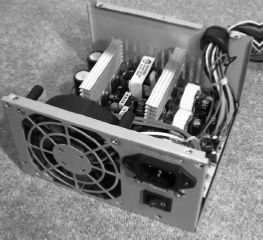
Figure 1: Power supply unit in a personal computer
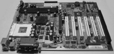
Figure 2: Personal computer motherboard
Three important power supply type can be integrated and employed in a power supply design that meets the final product electrical requirements.:
- Linear power supply design
- Switch power supply design
- High efficiency resonant and quasi-resonant technology switching power supplies.
Linear Power Supply Design
Linear power supply design are generally used in applications which don’t require high-efficiency, generate a low quantity of heat with low cost and short design time. These are very used in many applications where the output voltage is less than 40 volts DC. This technique permits to produce a single output voltage which is lower than the input voltage. the linear regulator provides an average efficiency of 35 to 50 per cent. However, the energy losses are dissipated as heat.
Switch Power Supply Design
Pulse Width Modulation (PWM) switching power supplies are more efficient (70 – 85% efficiency) and less heavy than linear regulators. They are mainly used in portable electronics products, small measurement instruments, automotive and aircraft products, off-line applications. PWM switching power supplies provide multiple output voltages with high efficiency. This type of power supplies dissipate less heat and need less heatsinking. However, PWM switching power supplies are more expensive and need more engineering development period.
High efficiency resonant technology switching power supplies
This technology is based on the PWM switching power supply. They are usually used in smaller size applications such as lightweight portable modules, spacecraft electronics and aircraft avionics. This power supply technology needs much more engineering design period and costs much more than the first two technologies.
Power Distribution
Generally, the electrical power is served through conductive coupling or electromagnetic coupling methods. In conductive coupling, power is delivered by electric conduction where charges travel from one body to another through a conductive medium such as electrochemical batteries and DC power supplies. In the electromagnetic coupling, the power is delivered through electromagnetic induction where the induced charges move by electromagnetic energy such as the wireless energy demonstration introduced by Nikola Tesla in1893 to illuminate vacuum bulbs.
Therefore, the power distribution network (PDN) which aims to provide the target device with a proper and stable voltage is achieved by the interconnection and combination of electrical devices which transfer the electrical power from a source to an electrical load with minimal energy loss and minimal power degradation.
The actual DC power supplies with higher current, lower voltage and smaller voltage noise margin are designed to reduce resistance when the current flow by using rectifiers – mainly when the electrical energy is derived from an AC source- which make the electrical current flows unidirectionally. This rectifier’s DC output in some cases needs further conditioning by using filters and decoupling devices (capacitors and inductors) due to AC voltage waveform variations from zero to peak amplitude.
Nowadays, the integrated power distribution is a new method in which both power conversion and distribution are embedded with load circuits. This new technique has enormous advantages by reducing the interconnection lengths between power conversion and load components which lead to minimizing the energy losses. PDN model is represented by Figure 3 from Voltage Resource Manager (VRM) to the Application Processor (AP).
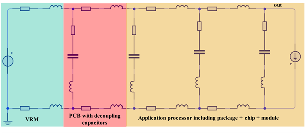
Figure 3: Power Delivery Network model
Therefore, PDN performances should be determined early in the PCB design by extracting the capacitor loop inductance, DC resistivity and target impedance decoupling parameter.
The capacitor loop inductance parameter helps to determine the decoupling capacitor as shown in Figure 4.
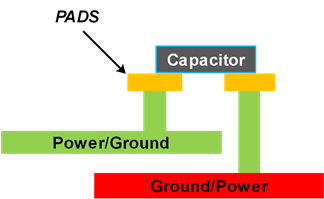
Figure 4: Loop inductance principle
The DC resistance can be determined by the net geometry and its material conductivity as depicted in Figure 5.
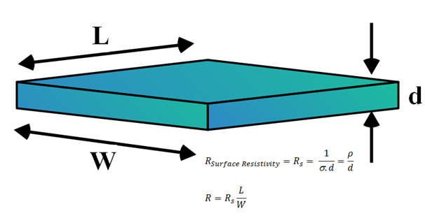
Figure 5: DC resistance
Therefore, the PDN analysis requires the calculation of the power net target impedance Ztarget by using the Frequency Domain Target Impedance Method (FDTIM) according to the following equation:
Power Integrity (PI)
The power integrity is a technic which leads to bring the power supply to its ideal or to make a constant and stable desired voltage supply regardless of power input changes and load power consumption.
In DC devices, an ideal power supply should maintain a constant output voltage regardless of load power consumption. Generally, the practical power supply features lead to the deviation of the output voltage from the ideal curve. Today, the PI can be integrated into the chip, in the printed circuit board (PCB), in the chip package and the main system.
To achieve power integrity at the PCB level, you should resolve the following four issues:
First of all, you must maintain and minimize the voltage ripple at the chips pads according to the specification established by the client.
Then, you should control the ground bounce and the electromagnetic interference due to the power distribution network which involves many conductors on the PCB that increase the noise. Also, you have to maintain the suitable DC voltage at the load when dealing with high currents.
Power Budget Calculation
Similarly to a budget that you need for your finances, a power budget indicates the necessary amount of energy that will supply the device exactly by its electronics modules and subsystems.
During the product design, power sizing and estimation permits to identify which power supply is more suitable for your product and also your component packages to larger dissipate heat.
In this case, we will take a simple example of an electronic schematic which requires a spreadsheet program (using Minitab 17) that includes simple math functions as shown in Figure 6 and datasheets of different ICs to learn how the power budget is calculated.

Figure 6: Power budget
The two columns (A and B) are employed to identify the data of each device. Then, the second two columns (C and D) can be used to calculate the multiplicative factor which means that if your circuit includes 6 components that hold 3 operational amplifiers (op-amps) per, then that will consume 18 times the power of a single device on the board that contains one op-amp per only. The next two columns (E and F) indicates the amount of current consumed by each device (indicated in the datasheet) and then the sum of all the devices on the board. Therefore, the supply voltage is indicated in column G which is used to compute the power consumption using the famous power formula (Power [W] =current [A] x voltage [V]) represented in column H per device. All these consumptions are summed and the total electrical power needed input to the product is given.
In the above example, the product requires 5 volts and 1 ampere from the power supply (~5 watts). In this case, it is suitable to design a power supply that is capable to provide 1.5 amperes. This 50 percent margin of error is considered as a cushion that permits to cover the miscalculation and expand the board in the future. This margin of error depends on the application and its requirements.
Power budgets are important while designing a new product because they give an idea about the battery life. For that reason, it is highly recommended to learn how to calculate the power budget and it will pay dividends for you in the future.
Regulated Power Supply Topology
A power supply which is based on linear regulators, converts and transforms unregulated alternating current (AC) to a constant and stable direct current (DC) even if either the load or input changes. This type of power supply consists of multiple blocks as shown in Figure 7.
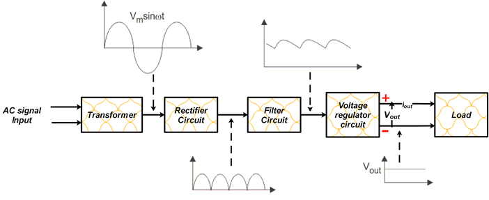
Figure 7: Linear regulated power supply block diagram
The linear power supply provides dielectric isolation by using a bulk power supply or an AC transformer. The regulation function permits the stability of the output voltage while load currents change. To simplify things, the linear regulators are step-down regulators only because the input voltage must be higher than the desired output voltage.
The stability of the output voltage in regulated power supplies is achieved by a closed negative feedback loop which permits to hold the output at a constant voltage value.
Two main consideration that you must take before dealing with linear regulators when designing a power supply. The first one is the headroom voltage which is the instantaneous voltage drop between the input and the output. The second consideration is the minimum dropout voltage of a linear regulator which is the minimum headroom voltage that the regulator can deal with, under this value, the regulators will fall out of regulation.
For example, the famous three-terminal regulators such as the LM78XX series, the dropout voltage is 1.8 to 2.5 volts DC. When designing linear power supplies where the input voltage is closer than 1.8 to 2.5 volts DC, it is highly recommended to use a low dropout regulator (LDO).
LDOs are linear voltage regulators that provide a very small voltage between the input and the output. They also continue to work even while the output voltage is closer to the input voltage. LDO takes a small place as compared to the ordinary linear voltage regulator and does not provide any switching noise. Some famous LDOs such as AMS1117, MIC29302, and RT9199 are presented in Figure
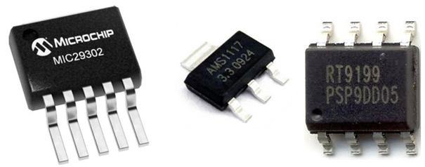
Figure 8: LDO ICs
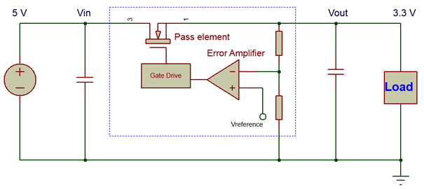
Figure 9: LDO composition
LDO consists of three main important components: pass element, reference voltage source and error amplifier as shown in Figure 9. The pass element is usually a P-channel /N-channel field-effect transistor (FET) or an NPN/PNP bipolar junction transistor (BJT). The input voltage is injected in the pass element (an N channel field effect transistor in this case). This FET works in the amplification /linear region to minimize the input voltage to the desired output voltage. The error amplifier follows the output voltage by comparing it to the reference voltage. LDOs can be employed in various consumer/personal electronics application mainly high-efficiency linear power supplies.
In the other hand, DC/DC converts are gaining ground fast and they can be included in power supplies. DC/DC converters convert an input DC voltage to a different DC voltage value by turning on and off (PWM) switching elements such as MOSFETs and FETs with high efficiency (95%). However, they provide ripples and switching noise in the output voltage which is not suitable for noise-sensitive products. It will be costly and difficult to design printed circuit boards (PCBs) using DC/DC converters because extra component must be added comparing to LDO regulators. As a PCB designer, it is important to choose the right technology that fit your requirements. In table 1, we compare between LDO regulators and DC/DC converters.
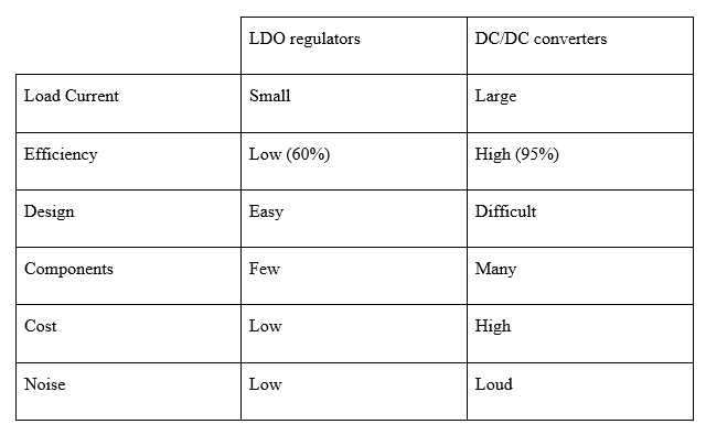
Table 1: Comparison between LDOs and DC/DC converters
Power Supply Design Guide
LDOs require capacitors at both the input and output. Therefore, the input capacitor bypasses the internal op-amp which is used in the voltage regulation loop. However, the output capacitor enhances the response of the regulator to sudden load changes. In general cases, you can put a 0.1 microfarads ceramic capacitor directly close to the LDO. When dealing with high current and using super LDO regulators (MIC5157 and MIC5158), you should use 10µF or larger capacitor. LDOs requires minimum capacitor value which is mentioned in the datasheet for the voltage control loop. To sum up, placing the bypass and filter ceramic capacitor is a solution for many unexpected problems.
In the other hand, the unwanted voltage drops and excessive lead resistance are solved by increasing conductor size as shown in Figure 10.
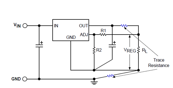
Figure 10: LDO circuit design
We will discuss in this section about regulators placement guidelines and we will focus on the popular TO-220 package but these recommendations will remain applicable to other packages.
LDOs should be placed at the top or at the top left of your board because they present the starting point of the signal that supplies your board.
When passing to the assembly process, you should employ pair of pliers to bend the outer lead of the LDO.
Your LDO TO-220 package may not require a heat sink if the power dissipation is not higher than 2 watts. Otherwise, you can use heat sinks with mounting clips which provides a low thermal resistance and a good heat contact area. Therefore, you can use machine screws for heat sink fixation as shown in Figure 11 but you have to apply the proper torque to avoid cracking the IC.
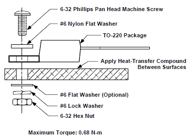
Figure 11: Mounting TO-220 package to Heat Sinks through machine screw
Power Supply Design – Practical example
Linear regulators are used in many portable applications to provide them with suitable voltage and current values. To more clarify ideas, we’ll take a practical example of mobile phone power supply design by calculating the power budget and then make power decisions.
Figure 13 presents a block diagram of the Openmoko Neo Freerunner (revision A6) cellular telephone and Table 2 lists its main key components with their power consumption retrieved directly from datasheets.
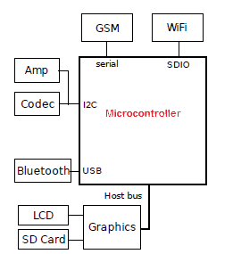
Figure 12: Freerunner device architecture
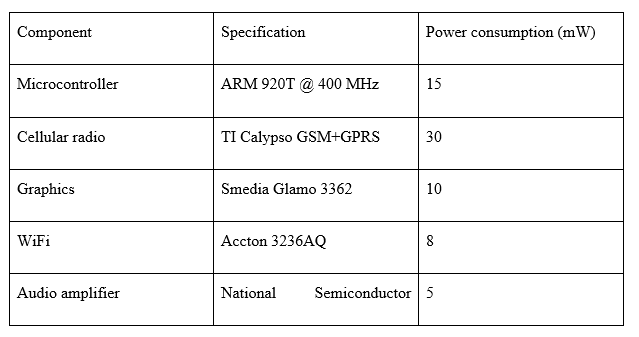
Table 2: the Openmoko Neo Freerunner module specifications
The power budget in this case is calculated automatically by summing the power consumptions of each device. The total will be 68 milliwatts.
To provide enough power to all these devices, we propose in this case to use LDOs and each module will have its power without disturbing others as shown in the Figure which represents the block diagram of the power supply (battery 200 milliamperes hour and 3.7 volts DC) to satisfy the power budget of the Openmoko Neo Freerunner smartphone.

Figure 13: Smartphone power supply block diagram


