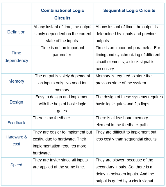
Difference between Sequential and Combinational Circuit
29/05/2022, hardwarebee
Digital logic circuits are broadly classified as combinational logic circuits and sequential logic circuits. Combinational circuits perform tasks that do not require memory to store their data — their operation is independent of time. The output at any instant of time is determined by the present inputs. The analysis of combinational logic is pretty straightforward: It involves a truth table, evaluation of logic expression and finally a circuit diagram.
Whereas sequential logic circuits have both a memory element and a combinational logic circuit. Their operation is dependent on time. The behavior of the system is determined by the inputs, outputs and the state of its memory. The steps involved in the analysis of sequential circuits include a state table, state diagram, evaluation of flip-flop equation and finally a circuit diagram.
In this article we will dig into difference between sequential and combinational circuit and understanding the difference between combinational and sequential circuit.
Combinational Logic Circuits
These are systems whose output at any instant of time is solely dependent on the present state of its inputs. These circuits are independent of the history of inputs and thus no need for a memory element (typically a flip flop). Also, their output is independent of the previous output.
A combinational circuit performs a specific operation, which is entirely determined by a truth table or a logic expression (a Boolean expression) or a logic circuit. These are the simple building blocks of digital systems and employ basic logic gates (AND, NAND, OR, NOR).
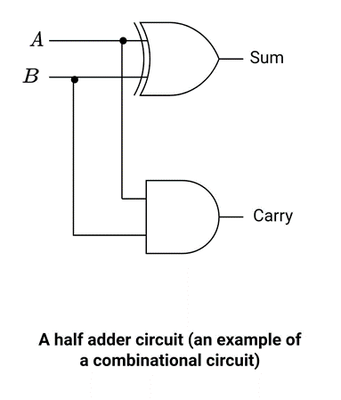
Below is a circuit of a half adder. It is a basic combinational circuit. There is no feedback path and no memory element.
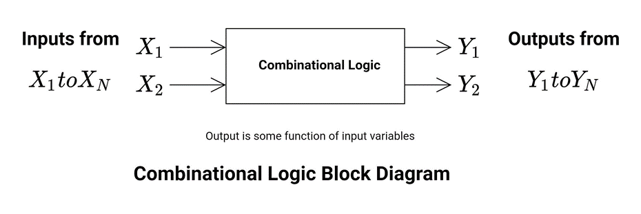
The following is a block diagram of the system. It may have any number of inputs and outputs depending on the operation to be performed. From the block diagram, the following points are concluded.
The output function can be expressed mathematically as follows:
![]()
Where,
Y1, Y2 …Ym are the output functions.
X1, X2 …Xm are the input functions.
- The block diagram shows a set of inputs and outputs. These inputs are processed by a memoryless logical network.
- The output exists as long as the input exists.
- The speed of the circuit depends on the propagation delay of individual gates. There is an inherent delay between the two gates.
- There is no need for a clock for the transition of states.
- There is no feedback path.
- They are less complicated than sequential circuits.
Design Process
- State the problem
- Identify inputs and outputs and determine the required number of inputs and outputs
- Assign a unique variable to each input and output
- Develop a truth table
- Simplify the SOP/POS expression with the help of Boolean algebra / K-map
- Implement each expression with the help of logic gates
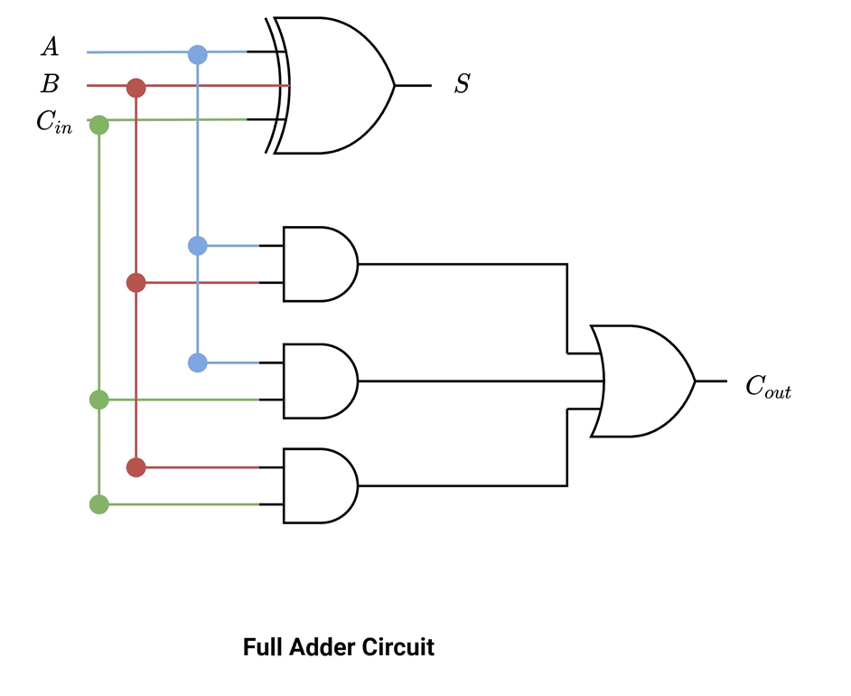
Example: 2-bit Full Adder Circuit
Step 1: To design a full adder. A full adder circuit adds two bits at a time. These two bits are added to the carry from the previous significant position.
Step 2: It is desirable to design a 2-bit full adder. This full adder circuit must be capable of adding the carry input as well. So, there are three inputs and two outputs. The first output is a sum and the other is “carry out”.
Two inputs are named A and B.
There is a third input carry input (Cin). There are two outputs sum (S) and carry out (Cout).
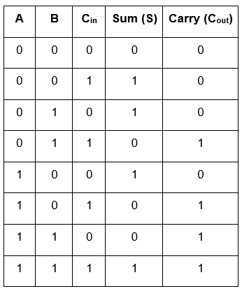
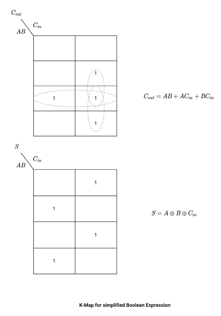
Step 4: The truth table is given below.
Step 5: Generate a K-map with the help of a truth table. The simplified full adder equation is obtained with the help of K-map.
Step 6:
Sequential Logic Circuits
As the name implies, these are circuits that are sequential. These are systems whose output at any instant is dependent on the present state of the inputs as well as the previous inputs of the system. As they are dependent on the previous state of the system, there is at least one memory element (flip flop), which can store the binary information within them. The state of the sequential circuit is the information stored in the memory at a given time. Their outputs are a function of the present inputs and the present state of the memory elements. To construct a sequential circuit, there must be a storage unit, which helps to retain information. The stored information is the history of outputs and can be recalled whenever needed. Flip flops are the basic building blocks for storage. There are many different flip-flops with different characteristics.
There are two different types of sequential circuits, synchronous (all the memory elements are clocked) and asynchronous (those sequential circuits that do not employ a clock for their operation). Most digital systems are based on synchronous circuits because the design and operation of clocked circuits are relatively easier than un-clocked sequential circuits.
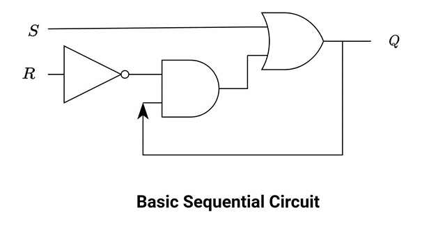
Below is a simple example of a sequential circuit. There is a feedback path between input and output.
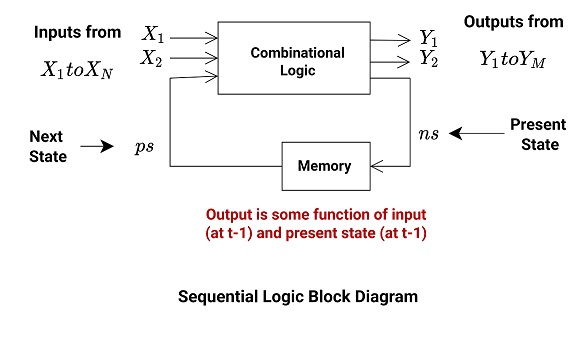
Block Diagram
The block diagram shows the same combinational logic circuit block along with a memory element. It is clear that memory also plays a role in determining the output for any given input.
The next state equation is a function of inputs and present states and is given as.
![]()
The output is a function of input and present state.
![]()
In some cases output is a function of the present state only. In this case,
![]()
In both cases, the output is associated with the present state.
From the block diagram following points are concluded:
- There is a set of inputs (X1, X2 …Xn) and a set of outputs (Y1, Y2 …Yn). The inputs are processed by a combinational circuit and stored in a memory element.
- Output is feedback to input and along with present inputs takes part in the next state output.
- State of the circuit means data stored in the memory element.
- The storage elements used in sequential circuits are called flip-flops. A flip-flop is a binary storage capable of storing 1 or 0 (it stores one bit only).
- Flip-flops receive their input from combinational circuits and also from the clock signal in the form of pulses that occur at fixed intervals of time (the clock is for synchronous sequential circuits).
- These circuits are complicated in design and their operation is difficult.
Design Process
The following steps are involved:
- Understand the given task which is usually a verbal description of the behavior of the circuit
- Draw a basic block diagram
- Obtain a state table or state diagram from the information obtained in steps 1 and step 2.
- Assign binary codes to the states. Assign each state a unique code (like 00, 01, 10.. etc)
- Choose the type of flip-flop. From the state, the table derives flip-flop input and output equations. The equations should be simplified.
- Draw the circuit
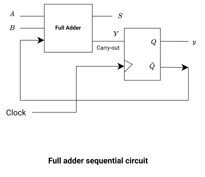
Example: a Full Adder Circuit
Step 1: To design a full adder circuit. It is capable of adding two unsigned numbers A and B. Output S depends on both the inputs and state as well.
Step 2: There are two possible states. SO and S1.
Step 3:
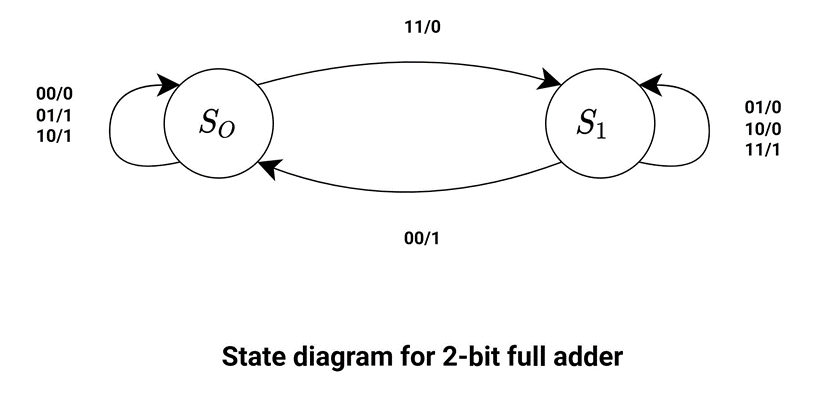
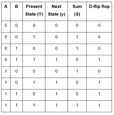
Step 4:
SO when present state = 0
S1 when present state = 1
Step 5: A single flip-flop can represent both states. For the implementation of a sequential circuit, let’s consider a D flip-flop. Carry is the input of the D flip-flop. It is stored for the next stage in this flip-flop.
Step 6:
Difference between Sequential and Combinational Circuit
Combinational circuit
At any instant of time, the output is only dependent on the current state of the inputs. Time is not an important parameter. The output is solely dependent on inputs only. No need for memory (flip flop). Easy to design and implement with the help of basic logic gates. There is no feedback. They are easier to implement but costly, due to hardware. Their implementation requires more hardware. They are faster since all inputs are applied at the same time.
Sequential circuit
At any instant of time, the output is determined by inputs and the previous outputs. Time is an important parameter. For timing and synchronizing of different circuit elements, a clock signal is necessary. Memory is required to store the previous state of the system. The design of these systems requires basic logic gates and flip flops. There is at least one memory element in the feedback path. They are difficult to implement but less costly than sequential circuits. They are slower, because of the secondary inputs. So, there is a delay in between inputs. And the output is gated by a clock signal.